Semiconductor device and manufacturing method thereof

a technology of semiconductors and manufacturing methods, applied in the direction of transistors, optics, instruments, etc., can solve the problems of poor coverage, complicated tft manufacturing, and fear of film being cut at a step

Inactive Publication Date: 2002-11-21
SEMICON ENERGY LAB CO LTD +1
View PDF64 Cites 82 Cited by
  • Summary
  • Abstract
  • Description
  • Claims
  • Application Information

AI Technical Summary

Problems solved by technology

With the use of one photomask, the steps of resist application, prebaking, exposure, development, postbaking and the like, the preceding and following steps of forming a coating film, etching and the like, and, furthermore, the step of resist removal, washing and drying, are inevitably added to complicate the manufacture of the TFT.
In the respective etchings in the comparative example, a side etching (an undercut...

Method used


Image

  • Semiconductor device and manufacturing method thereof
  • Semiconductor device and manufacturing method thereof
  • Semiconductor device and manufacturing method thereof

Examples


embodiment mode 2

[0107] First, a conductive film is formed on the entire surface of a substrate. The conductive film is formed into a desired shape through a first photolithography step. Later, the conducive film is etched to form a gate electrode or a gate wiring or a storage capacitance wiring.

[0108] Next, an insulating film is formed on the entire surface of the conductive film. Later, the insulating film functions as a gate insulating film. A first amorphous semiconductor film and a second amorphous semiconductor film containing an impurity element with one conductivity type (n-type or p-type) and a conductive film comprising metallic material (metallic material containing Al, Ti, Mo, Cu, Ta, Cr, Ni or Mo as a main component) are deposited on the insulating film.

[0109] Then, an unnecessary portion of the layered film formed of the first amorphous semiconductor film and the second amorphous semiconductor film containing an impurity element with one conductivity type (n-type or p-type) and the con...

embodiment 1

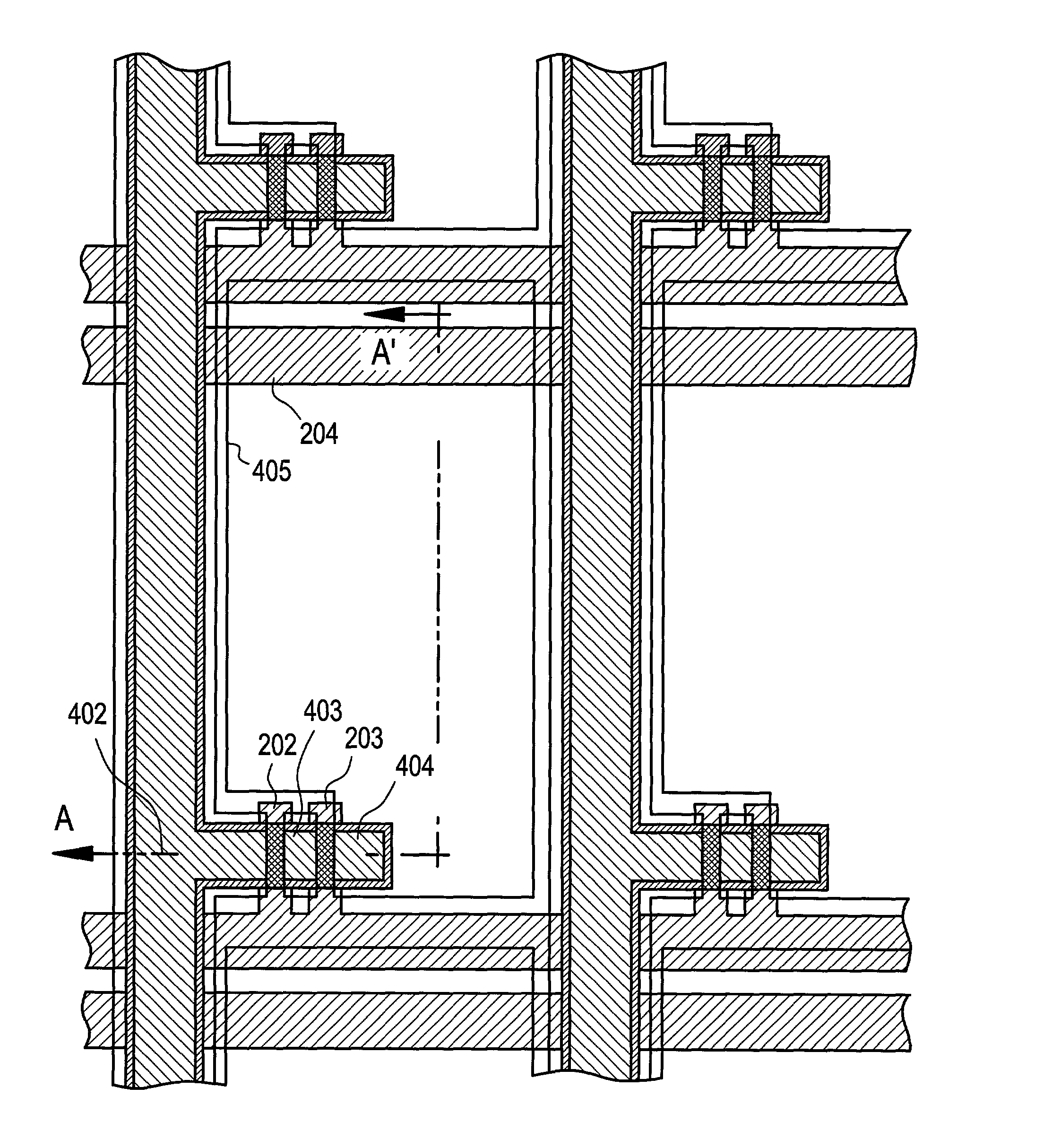
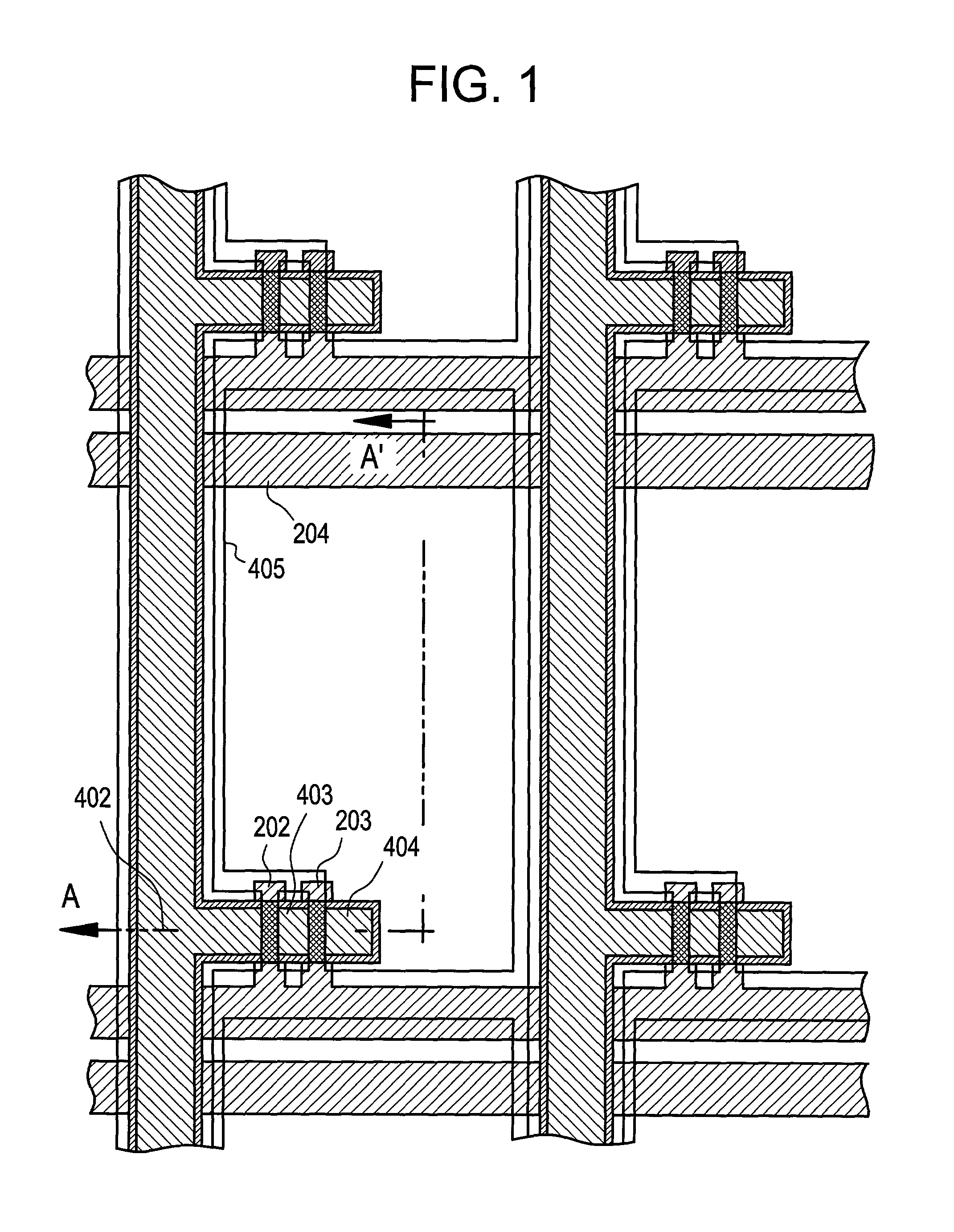
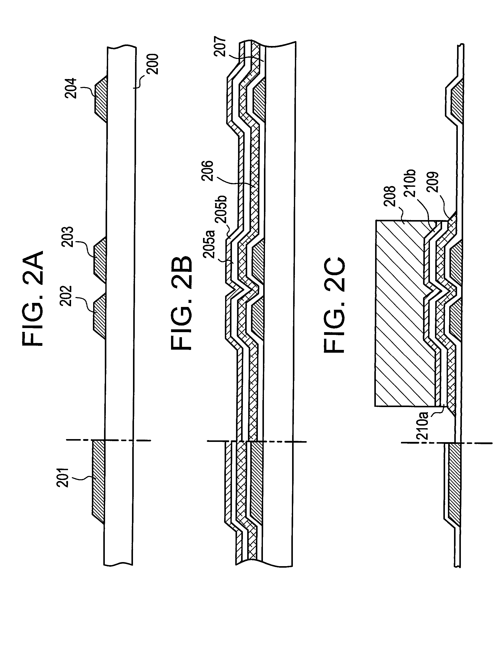
[0115] Embodiment 1 of the present invention will be described with reference to FIGS. 1 to 4B. In Embodiment 1, a manufacturing method of a liquid crystal display device is described. A method of manufacturing an inverse-stagger TFT in a pixel portion on a substrate and manufacturing a storage capacitor to be connected to the TFT will be described in detail in the order of the manufacturing steps. In FIGS. 2A to 4B, a terminal portion, which is provided at the end of the substrate so as to be electrically connected to a wiring of a circuit provided on another substrate, is also illustrated in the steps of manufacturing a TFT. The cross-sectional views of FIGS. 2A to 4B correspond to the cross section taken along a line AA-A' in FIG. 1.

[0116] First, a display device is manufactured by using a substrate 200 with light transmittance. As the substrate 200, a glass substrate such as barium borosilicate glass and alumino borosilicate glass, as represented by #7059 glass and #1737 glass m...

embodiment 2

[0134] The semiconductor display device including the channel etch type TFT in the pixel portion has been described in Embodiment 1, while a semiconductor display device including a channel stop type TFT in the pixel portion will be described in Embodiment 2 with reference to FIGS. 5A to 7C.

[0135] First, a semiconductor display device is manufactured by using a substrate 500 with light transmittance. As the substrate 500, a glass substrate such as barium borosilicate glass and alumino borosilicate glass, as represented by #7059 glass and #1737 glass manufactured by Corning Inc., can be used. Besides, a light transmitting substrate such as a quartz substrate and a plastic substrate can also be used as the substrate 500.

[0136] After forming a conductive film on the entire surface of the substrate 500, a first photolithography step is conducted to form a resist mask. An unnecessary portion is removed by etching to form gate electrodes 502 and 503, a storage capacitor wiring 504, and a ...


PUM


Abstract

The present invention has an object to provide an active-matrix liquid crystal display device that realizes the improvement in productivity as well as in yield. In the present invention, a laminate film comprising the conductive film comprising metallic material and the second amorphous semiconductor film containing an impurity element of one conductivity type and the amorphous semiconductor film is selectively etched with the same etching gas to form a side edge of the first amorphous semiconductor film 1001 into a taper shape. Thereby, a coverage problem of a pixel electrode 1003 can be solved and an inverse stagger type TFT can be completed with three photomask. Selected figure is FIG. 15.

Description

[0001] 1. Field of the invention[0002] The present invention relates to a semiconductor device including a semiconductor circuit constituted of a thin-film transistor (hereinafter, abbreviated as a TFT) and a manufacturing method thereof. More particularly, the present invention relates to an electro-optical device as represented by a liquid crystal display panel and an electronic device including such an electro-optical device as a constituent.[0003] Throughout the specification, the term "semiconductor device" indicates all devices that utilize the semiconductor characteristics to function; electro-optical devices (hereinafter, referred to as display devices), semiconductor circuits and electronic devices are all included in the category of the semiconductor devices.[0004] 2. Description of the Related Art[0005] Recently, there has been developed a technique for manufacturing a TFT by using a thin semiconductor film (with a thickness of about hundreds to thousands of nm) formed on...

Claims


Application Information

Patent Timeline
IPC IPC(8): G02F1/1368H01L21/336H01L21/77H01L21/84H01L27/12H01L29/06H01L29/786
CPCG02F1/1368H01L29/06H01L29/66765H01L27/1288H01L29/78669H01L27/124H01L27/1244H01L29/78621
Inventor SUZAWA, HIDEOMIKUSUYAMA, YOSHIHIROYAMAZAKI, SHUNPEI
Owner SEMICON ENERGY LAB CO LTD
Why Eureka
Try Eureka