

Fused polynuclear compound and organic luminescence device
a technology of luminescence device and polynuclear compound, which is applied in the direction of organic semiconductor device, other domestic articles, natural mineral layered products, etc., can solve the problems of insufficient color purities, change in luminance, and accompanied luminescence device durability
- Summary
- Abstract
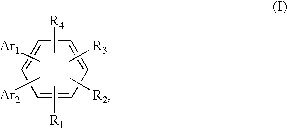
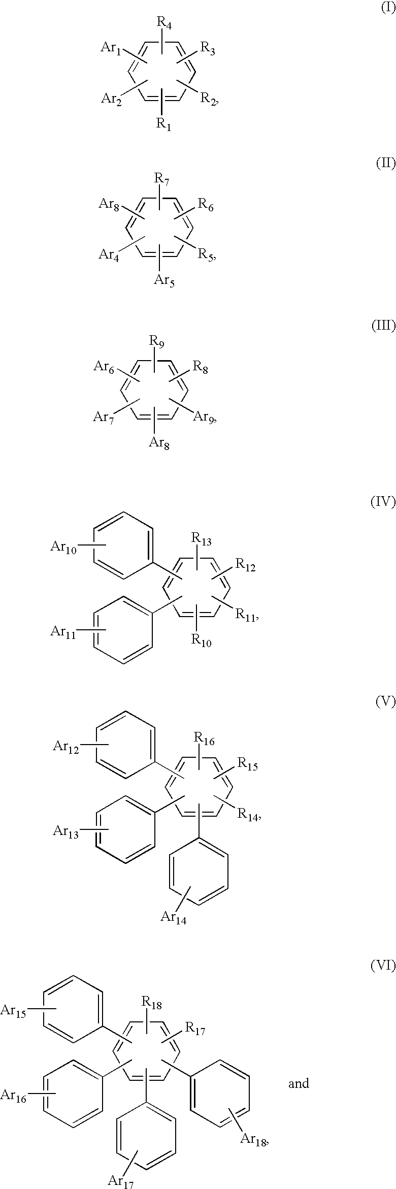
- Description
- Claims
- Application Information
AI Technical Summary
Benefits of technology
Problems solved by technology
Method used
Image

Examples
example 1
[0081] An organic luminescence device shown in FIG. 2 was prepared in the following manner.
[0082] On a 0.7 mm-thick glass substrate 1, a 120 nm-thick ITO (indium tin oxide) film (anode 2) was formed by sputtering to prepare a transparent electroconductive support, which was then successively subjected to ultrasonic cleaning with acetone and with isopropyl alcohol (IPA). The resultant transparent electroconductive support was then subjected to boiling leaning with IPA and was dried, followed by UV / ozone cleaning.
[0083] On the transparent electroconductive support, a solution of a hole transport material shown below in chloroform was applied by spin coating to form a 30 nm-thick hole transport layer 5. 13
[0084] On the hole transport layer 5, a 50 nm-thick electron transport layer 6 of a fused polynuclear compound (Ex. Comp. No. 1) was formed by vacuum deposition under conditions including a vacuum degree (pressure) of 1.0.times.10.sup.-4 Pa and a deposition rate of 0.2-0.3 nm / sec.
[008...
examples 2-15
[0088] Organic luminescence devices were prepared and evaluated in the same manner as in Example 1 except that the fused polynuclear compound (Ex. Comp. No. 1) was changed to those (Ex. Comp. Nos. 5, 10, 16, 19, 24, 25, 31, 36, 39, 43, 46, 51, 58 and 63), respectively.
[0089] The results are shown in Table 1.
example 16
[0093] An organic luminescence device shown in FIG. 3 was prepared in the following manner.
[0094] In a similar manner as in Example 1, on a transparent electroconductive support, a 120 nm-thick ITO film (anode) and a 30 nm-thick hole transport layer 5 were formed.
[0095] On the hole transport layer 5, a 20 nm-thick luminescence layer 3 of a fused polynuclear compound (Ex. Comp. No. 4) was formed by vacuum deposition (1.0.times.10.sup.4 Pa;0.2-0.3 nm / sec).
[0096] On the luminescence layer 3, a 40 nm-thick electron transport layer 6 of tris-(8-hydroxy-quinoline)aluminum (Alq3) was formed by vacuum deposition (1.0.times.10.sup.-4 Pa;0.2-0.3 nm / sec).
[0097] Then, on the electron transport layer 6, a 150 nm-thick metal electrode (cathode 4) of an aluminum-lithium alloy (Li content: 1 atomic %) was formed by vacuum deposition (1.0.times.10.sup.-4 Pa;1.0-1.2 nm / sec).
[0098] To the thus-prepared organic luminescence device, a DC voltage of 8 volts was applied between the ITO electrode (anode 2,...
PUM
| Property | Measurement | Unit |
|---|---|---|
| Length | aaaaa | aaaaa |
| Length | aaaaa | aaaaa |
| Length | aaaaa | aaaaa |
Abstract
Description
Claims
Application Information