Organic light-emitting device

a light-emitting device and organic compound technology, applied in the direction of discharge tube luminescnet screens, natural mineral layered products, other domestic articles, etc., can solve the problems of low emission efficiency of the device, insufficient durability life, and insufficient emission efficiency and durability life. achieve excellent stability over time, high luminance and efficiency

Inactive Publication Date: 2011-05-31
CANON KK
View PDF42 Cites 1 Cited by
  • Summary
  • Abstract
  • Description
  • Claims
  • Application Information

AI Technical Summary

Benefits of technology

[0016]It is, therefore, an object of the present invention to provide an organic light-emitting device having an optical output with a high efficiency, a high luminance and a long life.
[0030]The present invention can provide an organic light-emitting device which has extremely high luminance and efficiency, and excellent stability over time.

Problems solved by technology

However, there still remain a large number of problems in terms of durability such as a change over time due to long-term use and deterioration due to an atmospheric gas containing oxygen or to moisture.
The publication describes that such compound can form a good organic film because of its low crystallinity particularly when used for a blue-light-emitting material or an electron-injecting / transporting material, but the emission efficiency and durability life have not practically been sufficient.
The publications describe that those anthracene derivatives provide green light emission when used as a light-emitting material, but when used to make a device, the emission efficiency of the device has been low and the durability life of the device has not practically been sufficient.
H11-8068 discloses that a device using a particular anthracene compound containing an olefin moiety for a light-emitting material shows light emission of yellow to red color range, but the emission efficiency has not been practically sufficient.
The patent describes that a red-light-emitting device with improved reliability is obtained, but the emission efficiency is not practically sufficient and it is difficult to emit blue light because of its device structure.
Japanese Patent Application Laid-Open No. 2002-324678 discloses that an organic light-emitting device using a material which has a pyrene-substituted benzene ring has good emission characteristics and durability, but the external quantum efficiency of the device is low, and the patent has no specific description about the durability life.

Method used


Image

  • Organic light-emitting device
  • Organic light-emitting device
  • Organic light-emitting device

Examples


example 1

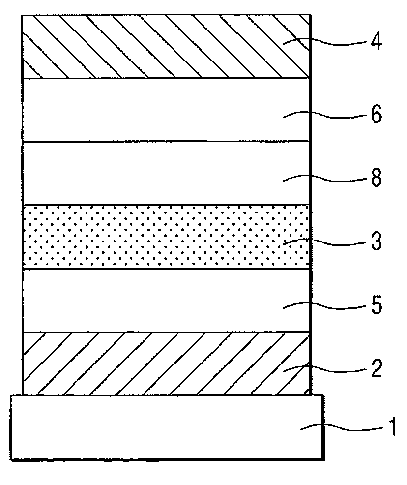
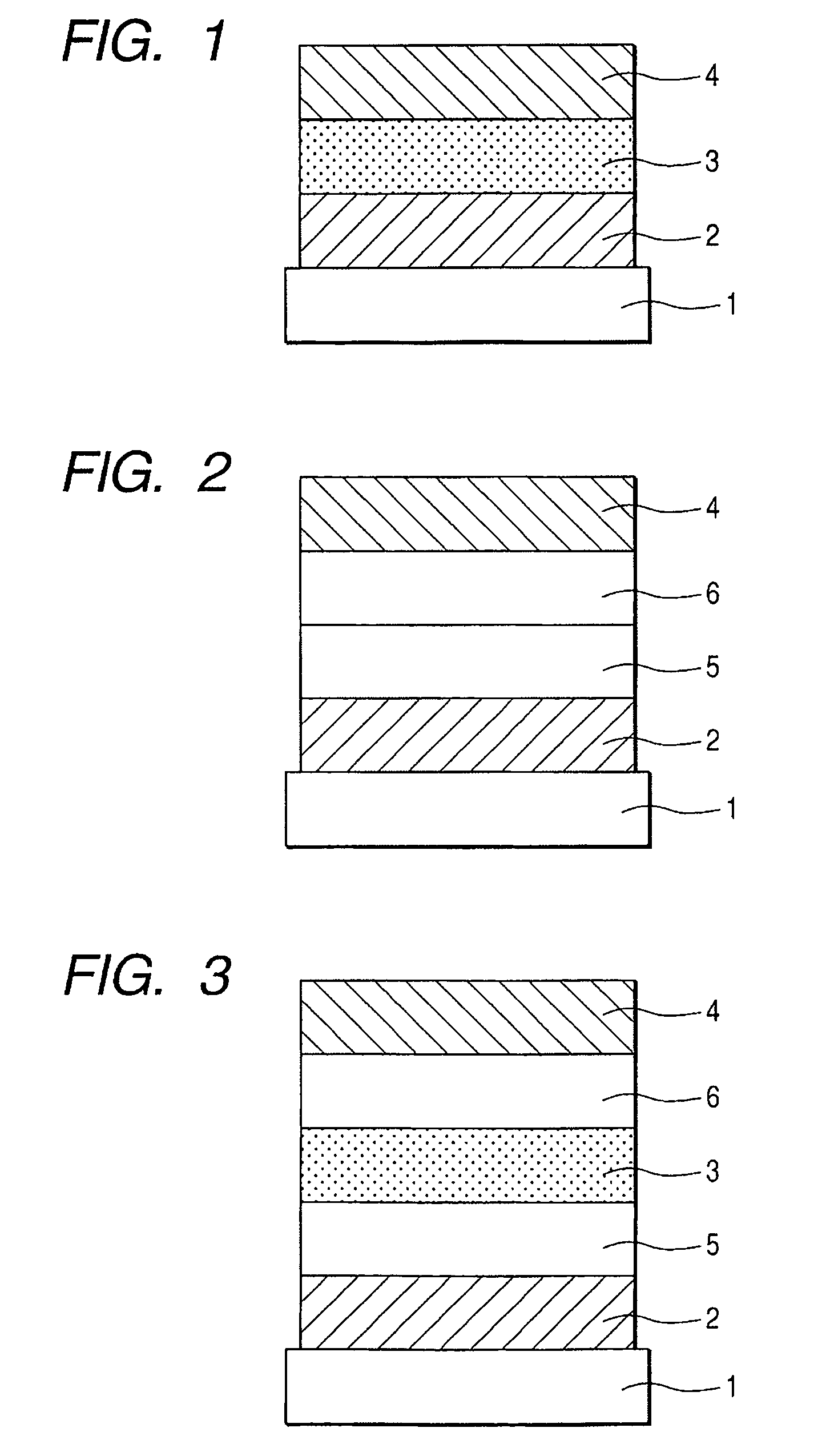
[0104]An organic light-emitting device having a structure shown in FIG. 3 was prepared with a method described below.

[0105]A transparent conductive support substrate was prepared which had a film of indium tin oxide (ITO) with a thickness of 120 nm as an anode 2 formed on a glass substrate 1 by a sputtering method. The transparent conductive support substrate was ultrasonically cleaned sequentially with acetone and isopropyl alcohol (IPA), subsequently cleaned with boiled IPA, was dried, was further cleaned with UV / ozone, and was used.

[0106]A chloroform solution of a compound represented by the following structural formula, which was a hole-transporting material, was prepared so that the concentration became 0.2 wt. %.

[0107]

[0108]The solution was dropped on the above described ITO electrode and spin-coated at first for ten seconds at a rotation speed of 500 RPM and then for one minute at a rotation speed of 1,000 RPM, to form a film. The substrate was dried in a vacuum oven at 80° C...

examples 2 to 4

[0116]Devices were prepared by following the same procedure as in Example 1 with the exception that the exemplified compound No. 3 was used as the first compound and the compounds shown in Table 1 below were used as the second compound, and were similarly evaluated. The results are shown in Table 1.

[0117]

TABLE 1ExemplifiedcompoundNo. ofAppliedExamplesecondvoltageLuminanceEfficiencyNo.compound(V)(cd / m2)(lm / W)21074.021801132014.030501242024.0138011

[0118]Any device of Examples 2 to 4 emitted a green light having a peak wavelength in the vicinity of 520 nm originating from the exemplified compound No. 3.

[0119]In addition, the absorption spectra in ultraviolet to visible light region were measured on the devices, and as a result, the second compounds each had a larger bandgap than the first compound had in any Example.

examples 5 to 8

[0120]Devices were prepared by following the same procedure as in Example 1 with the exception that the exemplified compound No. 5 was used as the first compound, the compounds shown in Table 2 below were used as the second compound, the codeposition ratio at the time of forming the light-emitting layer was set to 25:75 (weight ratio), and 2,9-bis[2-(9,9-dimethylfluorenyl)]phenanthroline was used for the electron-transporting layer; and were similarly evaluated. The results are shown in Table 2.

[0121]

TABLE 2ExemplifiedcompoundNo. ofAppliedExamplesecondvoltageLuminanceEfficiencyNo.compound(V)(cd / m2)(lm / W)51014.07701261074.026001372014.036201482124.0162013

[0122]Any device of Examples 5 to 8 emitted a green light having a peak wavelength in the vicinity of 530 nm originating from the exemplified compound No. 5.

[0123]Furthermore, a voltage was applied to the device of Example 7 in nitrogen atmosphere for 100 hours so that the current density was kept at 30 mA / cm2. As a result, the devic...


PUM

PropertyMeasurementUnit
applied voltageaaaaaaaaaa
thicknessaaaaaaaaaa
thicknessaaaaaaaaaa

Abstract

An organic light-emitting device is provided which has an optical output with a high efficiency, a high luminance and a long life and which includes a pair of electrodes including an anode and a cathode, and at least one layer comprising an organic compound provided between the pair of electrodes, wherein at least one layer having a light-emitting region of the at least one layer comprising the organic compound comprises a first compound represented by the general formula (1):and a second compound having a bandgap larger than a bandgap of the first compound.

Description

BACKGROUND OF THE INVENTION[0001]1. Field of the Invention[0002]The present invention relates to a light-emitting device using an organic compound, and more particularly, relates to an organic light-emitting device which emits light by applying an electric field to a thin film comprising the organic compound.[0003]2. Related Background Art[0004]An organic light-emitting device is a device which forms excitons of a fluorescent organic compound by interposing a thin film comprising the fluorescent compound between an anode and a cathode and injecting electrons and holes (positive holes) from the electrodes, and utilizes light emitted when the excitons return to a ground state.[0005]In a study according to Eastman Kodak Corporation in 1987 (Appl. Phys. Lett. 51, 913 (1987)), it has been reported that a device having a function-separated two-layer structure, which uses ITO for an anode, an alloy of magnesium and silver for a cathode, an aluminum quinolinol complex for an electron-transp...

Claims


Application Information

Patent Timeline
Patent Type & Authority Patents(United States)
IPC IPC(8): H01L51/54C09K11/06
CPCC09K11/06H05B33/14H01L51/0058H01L51/006C09K2211/1011C09K2211/1014C09K2211/1029C09K2211/1044C09K2211/1048C09K2211/1088C09K2211/1092H01L51/0052H01L51/0054H01L51/5012C09K2211/1007Y10S428/917H10K85/622H10K85/626H10K85/633H10K85/615H10K50/11
Inventor OKINAKA, KEIJIYASHIMA, MASATAKASAITOH, AKIHITOYAMADA, NAOKISENOO, AKIHIROUENO, KAZUNORI
Owner CANON KK
Why Eureka
Try Eureka