Semiconductor device having an external electrode

a technology of a semiconductor device and an external electrode, which is applied in the direction of semiconductor devices, semiconductor/solid-state device details, electrical apparatus, etc., can solve the problems of reducing the bonding strength per solder bump, reducing the barrier function for preventing sn diffusion, and reducing the bonding strength

Inactive Publication Date: 2003-02-06
NEC ELECTRONICS CORP
View PDF6 Cites 70 Cited by
  • Summary
  • Abstract
  • Description
  • Claims
  • Application Information

AI Technical Summary

Problems solved by technology

The larger tensile stress causes a problem in that the process for forming a barrier metal film having a large thickness generates a crack in the wiring pad 12 or peel-off of the insulator film 14 underlying the barrier metal film.
However, the pillar crystalline structure reduces the path length for the Sn diffusion due to the straight crystalline boundary, thereby degrading the barrier function for preventing the Sn diffusion, which is undesirable.
In addition, the development of smaller dimensions for the solder bumps reduces the bonding strength per solder bump, and highlights the problem of the bonding strength that is reduced due to the presence of the passive Ni oxide film formed on the electrode Ni film 52 in the another conventional technique.

Method used


Image

  • Semiconductor device having an external electrode
  • Semiconductor device having an external electrode
  • Semiconductor device having an external electrode

Examples


first embodiment

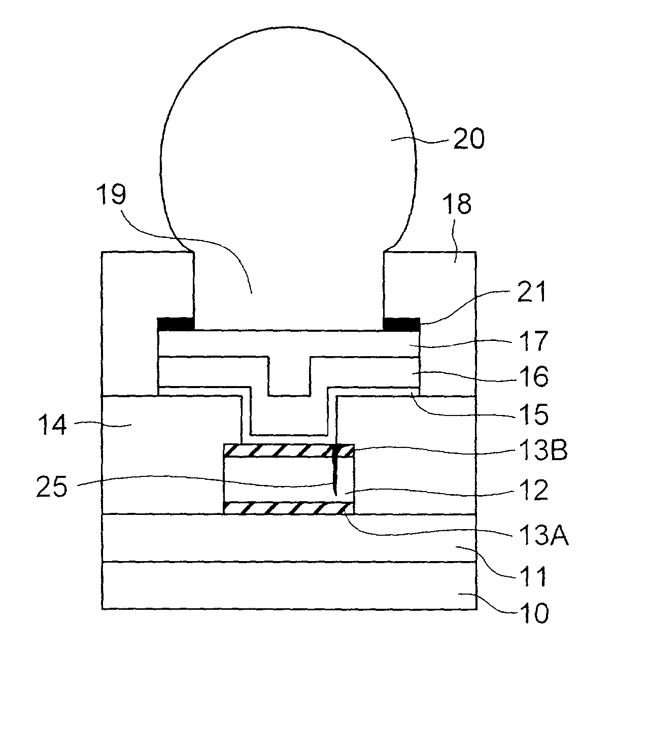
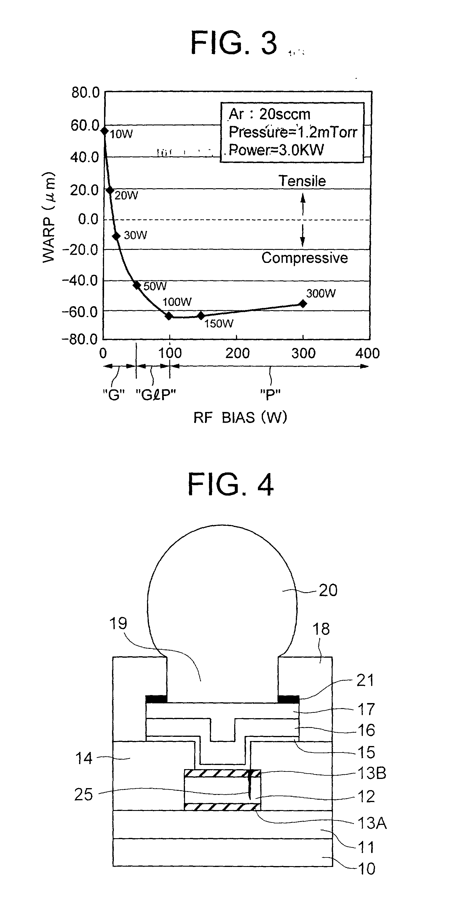
[0047] Referring to FIG. 4, an external electrode according to the present invention is formed on a dielectric film 11, which overlies a silicon substrate 10 with an intervention of a plurality of wiring layers and interlayer dielectric films (not shown). The external electrode includes a wiring pad 12 made of Al and formed on the dielectric film 11 with an intervention of an underlying TiN / Ti film 13A, which improves adhesion between the wiring pad 12 and the dielectric film 11 and thus improves reliability of the wiring structure. Another dielectric film 14 covering the wiring pad 12 has a two-layer structure including a silicon oxide (SiO.sub.2) layer and a silicon oxynitride (SiON) layer, which have a through-hole exposing the top of the wiring pad 12.

[0048] The top of the wiring pad 12 is coated with another TiN / Ti film 13B for improving the resistance against an electro-migration failure to improve the reliability of the wiring structure. A barrier metal electrode is formed on...

second embodiment

[0079] Referring to FIG. 14, an external electrode according to the present invention is similar to the external electrode shown in FIG. 4 except for the structure of the barrier metal electrode. More specifically, the barrier metal electrode shown in FIG. 14 includes an adherence Ti film 31 as a first conductive film, a sputtered Ni--V barrier metal film 32 as a second conductive film, a seed Cu film 33 as a third conductive film, a plating Ni barrier film 34 as a fourth conductive film, a solder-wetting Cu film 35 as a fifth conductive film, and an adherence Ti film 36 disposed between the solder-wetting Cu film 35 and the polyimide coat 18. The Ni--V barrier metal film 32 has a two-layer structure, such as shown in FIG. 5A, including a first barrier metal layer having a granular crystalline structure and a second barrier metal layer having a pillar crystalline structure.

[0080] In the structure of the second embodiment, the seed Cu film 33 overlying the sputtered Ni--V barrier met...

third embodiment

[0085] In the third embodiment, the adherence TiW film 40 acts as a protective layer which prevents the Sn component in the solder ball 20 mounted on the barrier metal electrode from diffusing toward the barrier metal electrode through the internal of the polyimide coat 18 and the interface between the conductive layers. The TiW film 40 has a lower reactivity with the solder, and thus is suited to this purpose.


PUM

PropertyMeasurementUnit
thicknessaaaaaaaaaa
thicknessaaaaaaaaaa
thicknessaaaaaaaaaa

Abstract

An external electrode in a semiconductor device includes, from the bottom of a wafer, a wiring pad, first and second barrier metal layers, a solder-wetting film and a solder ball. The first barrier metal layer has a tensile internal stress and a granular crystalline structure, whereas the second barrier metal layer has a compressive internal stress and a pillar crystalline structure. The two-layer structure of the barrier metal film has an excellent barrier function against Sn diffusion from the solder ball and reduces the internal stress of the barrier metal film.

Description

[0001] (a) Field of the Invention[0002] The present invention relates to a semiconductor device having an external electrode and, more particularly, to a semiconductor device having an external electrode including a barrier metal electrode.[0003] (b) Description of the Related Art[0004] In a semiconductor device, an external electrode is generally formed by mounting a solder ball on a wiring pad connected to the internal wiring in the semiconductor device, The solder ball is bonded onto a corresponding electrode of a wiring board such as a printed circuit board. The semiconductor device is connected to an external circuit via the wiring board by the external electrode including such a solder ball, and also mechanically fixed onto the wiring board.[0005] The semiconductor device generally includes a barrier metal electrode (electrode layer) interposed between the solder ball and the underlying wiring pad for preventing the tin (Sn) component in the solder ball from being diffused int...

Claims


Application Information

Patent Timeline
Patent Type & Authority Applications(United States)
IPC IPC(8): H01L21/285H01L21/3205H01L21/60H01L23/485H01L23/52
CPCH01L24/11H01L2224/0401H01L2224/13022H01L2224/13099H01L2924/01002H01L2924/01004H01L2924/01013H01L2924/01015H01L2924/01018H01L2924/01022H01L2924/01029H01L2924/01073H01L2924/01074H01L2924/01078H01L2924/01079H01L2924/01082H01L2924/01322H01L24/13H01L2924/01005H01L2924/01006H01L2924/01023H01L2924/01033H01L2924/014H01L2224/02166H01L2224/131H01L2224/10126H01L2924/0001H01L2224/05124H01L2224/05147H01L2224/05155H01L2224/05166H01L2224/05647H01L24/03H01L24/05H01L2924/00014H01L2924/013H01L2924/01014H01L21/60
Inventor MIKAGI, KAORUFURUYA, AKIRAHATANO, KEISUKE
Owner NEC ELECTRONICS CORP
Why Eureka
Try Eureka