Method for reducing line edge roughness of photoresist

a technology of photoresist and line edge roughness, which is applied in the direction of photomechanical equipment, instruments, and photosensitive material processing, etc., can solve the problems of non-uniform distribution of polymers which are composition of photoresist, non-smooth surface and line width variation, and limited practice in semiconductor fabrication, etc., to achieve the effect of reducing the roughness of the line edge of the photoresis

Inactive Publication Date: 2003-02-06
MACRONIX INT CO LTD
View PDF0 Cites 21 Cited by
  • Summary
  • Abstract
  • Description
  • Claims
  • Application Information

AI Technical Summary

Benefits of technology

0009] One main object of this invention is to effectively reduce line edge roughness of photoresist.

Problems solved by technology

Because practical semiconductor fabrication is limited by numerous factor, such as available materials of both photoresist and developer, unavoidable errors during both developing process and priming process, standing wave phenomena, and non-uniform distribution of polymers which are composition of photoresist.
Owing to location and number of trenches are random distributed, disadvantages such as non-smooth surface and line width variation are occurred and usually is called as line edge roughness. FIG. 1A and FIG. 1B illustrate ideal shape of patterned photoresist, and both FIG. 1C and FIG. 1D qualitatively show real shape of patterned photoresist while line edge roughness is happened.
However, because standing wave phenomena is unavoidable while photoresist is exposed by light and improvement is limited by available material of photoresist, conventional semiconductor fabrication could not effectively reduce, or even eliminate, line edge roughness of patterned photoresist.

Method used


Image

  • Method for reducing line edge roughness of photoresist
  • Method for reducing line edge roughness of photoresist
  • Method for reducing line edge roughness of photoresist

Examples


Embodiment Construction

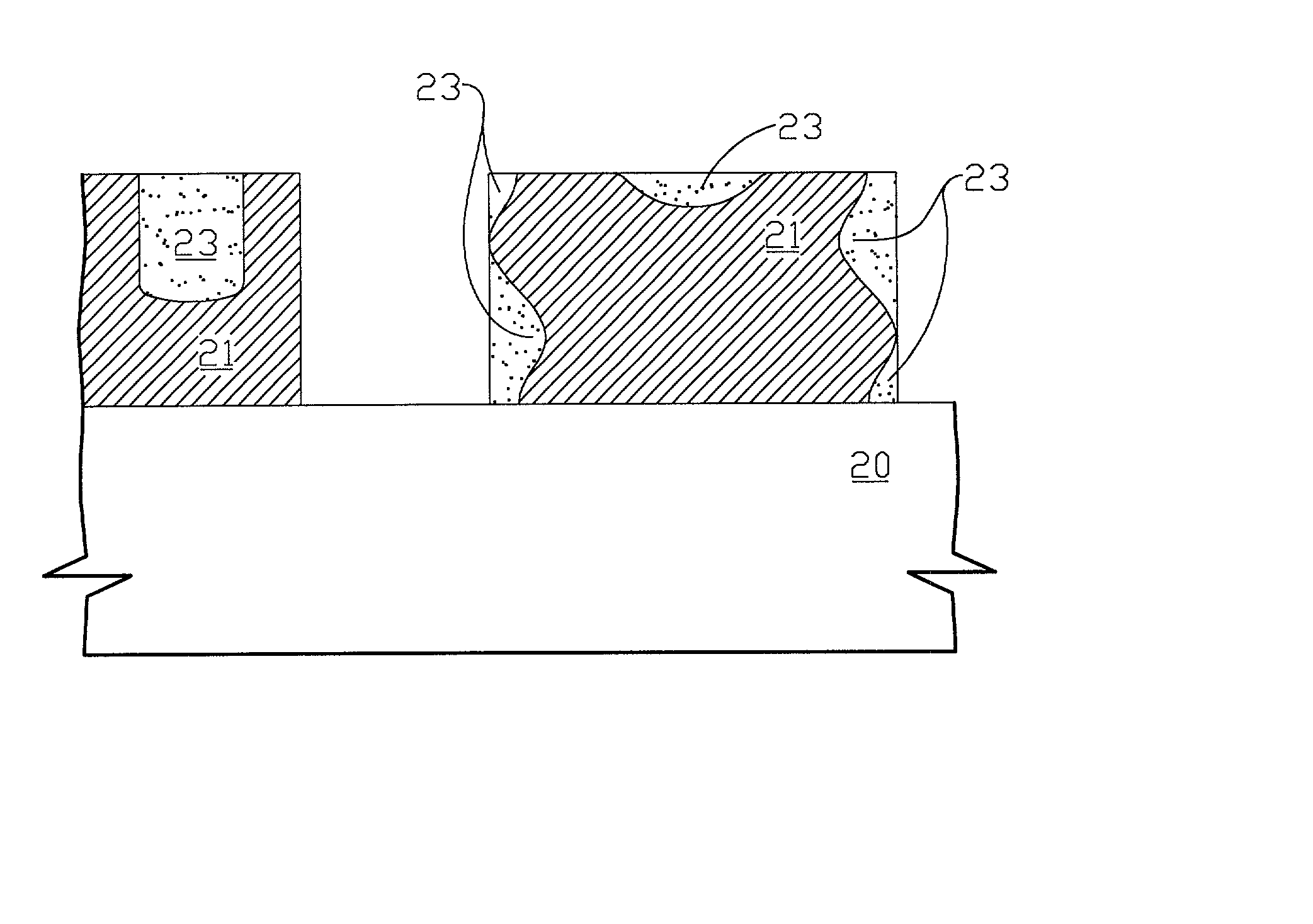
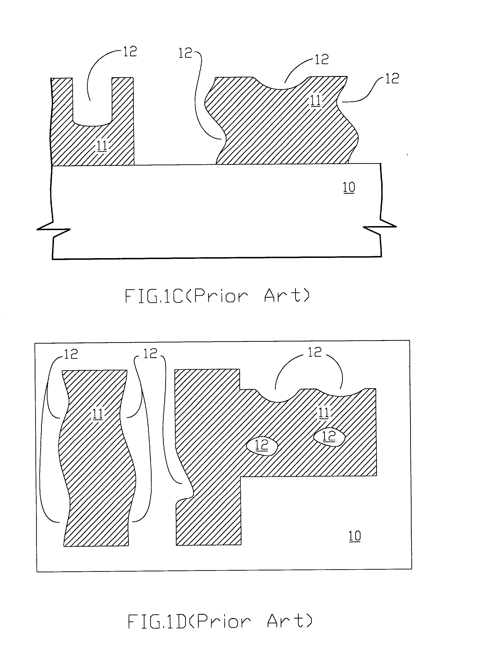
[0019] Because choice of photoresist material, baking time and baking temperature are strongly related to whole process for transferring pattern from mask into photoresist, none of them could be decided only in accordance with requirement for preventing line edge roughness. Thus, this present invention reduces line edge roughness of photoresist from another approach: First, still use conventional semiconductor fabrication to form photoresist pattern which has line edge roughness such as trenches, non-smooth surface, and line width variation. Then, after pattern is transformed into photoresist, fills trenches (include holes) in photoresist by an additional material, so let non-smooth surface and line width variation are reduced or even eliminated. Finally, uses both photoresist and additional material as a mask to transfer pattern into semiconductor substrate.

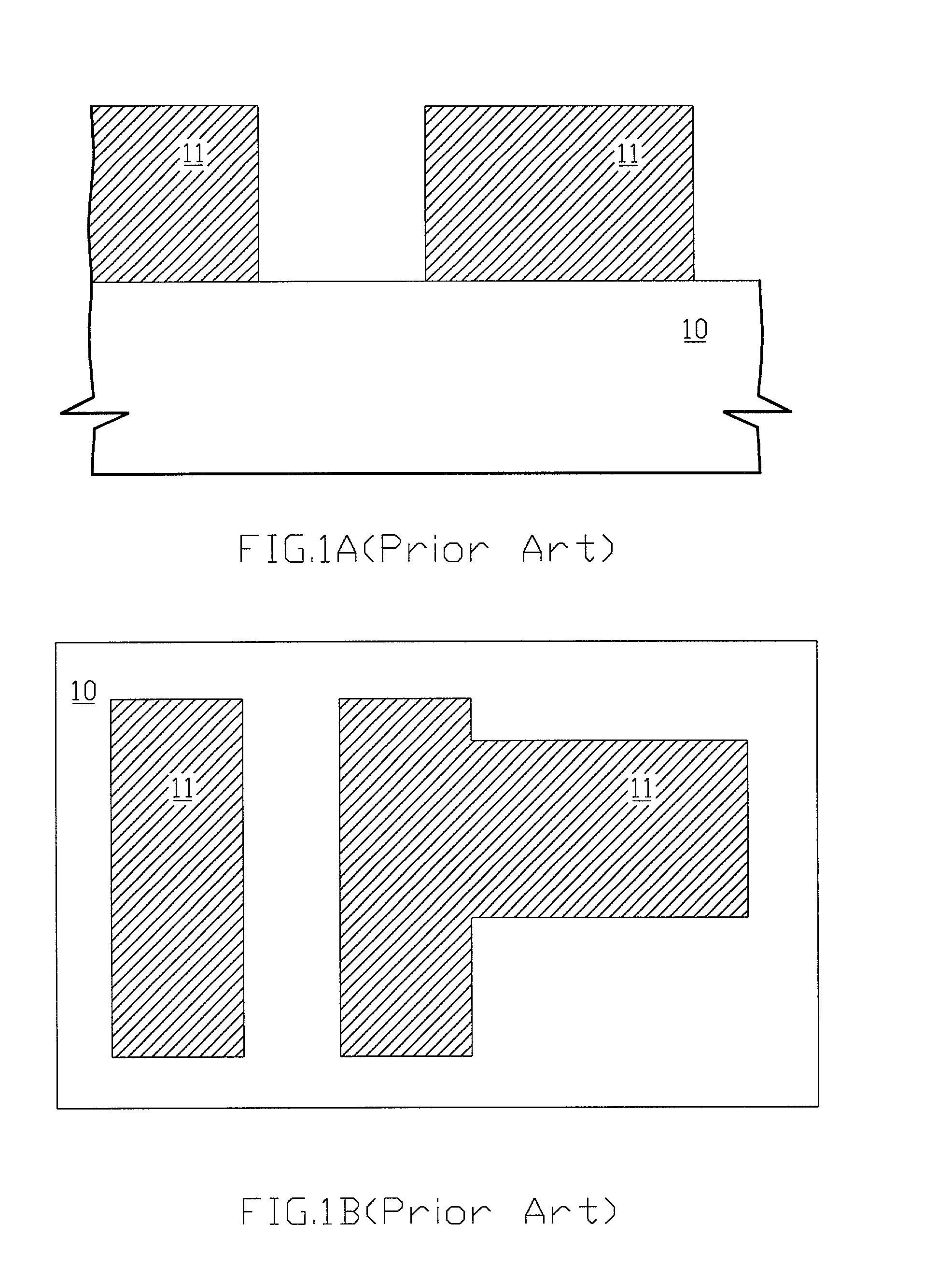
[0020] In short, conventional semiconductor fabrication usually directly uses photoresist as the mask used by etch process and...


PUM

PropertyMeasurementUnit
roughnessaaaaaaaaaa
thermosettingaaaaaaaaaa
thermoplasticityaaaaaaaaaa

Abstract

A method for reducing line edge roughness of photoresist, at least include: provide a photoresist which at least has a trench and is located on substrate; fill trenches so let that trenches are totally filled by an additional material; remove part of additional material which is located on photoresist and substrate; and treat additional material so let that adhesion between additional material and photoresist is enhanced after additional material is treated. Moreover, while only trenches are filled by additional material, step of removing part of additional material could be omitted; while adhesion between additional material and photoresist is good, step of treating additional material could be omitted.

Description

BACKGROUND OF THE INVENTION[0001] 1. Field of the Invention[0002] This invention relates generally to method for reducing line edge roughness of photoresist, and particularly relates to method for improving precision of pattern of photoresist without changing photoresist material or changing both develop process and bake process.[0003] 2. Description of the Prior Art[0004] For semiconductor fabrication, photoresist is an indispensable part for transferring pattern of mask into semiconductor substrate. Because pattern of photoresist essential is pattern of semiconductor substrate, how to ensure pattern of photoresist is equal to pattern of mask is an important key for whether pattern is accurately transferred.[0005] Because practical semiconductor fabrication is limited by numerous factor, such as available materials of both photoresist and developer, unavoidable errors during both developing process and priming process, standing wave phenomena, and non-uniform distribution of polyme...

Claims


Application Information

Patent Timeline
Patent Type & Authority Applications(United States)
IPC IPC(8): G03F7/40
CPCG03F7/40Y10S430/143
Inventor LU, YEN-TING
Owner MACRONIX INT CO LTD
Why Eureka
Try Eureka