

Semiconductor device and method for manufacturing the same
a semiconductor and device technology, applied in semiconductor devices, semiconductor/solid-state device details, electrical apparatus, etc., can solve problems such as wiring reliability and migration resistance reduction, deformation of wiring layers, and failure of embossed components
- Summary
- Abstract
- Description
- Claims
- Application Information
AI Technical Summary
Benefits of technology
Problems solved by technology
Method used
Image

Examples
Embodiment Construction
[0032] One exemplary embodiment of the present invention will be described below with reference to the accompanying drawings.
[0033] [Device]
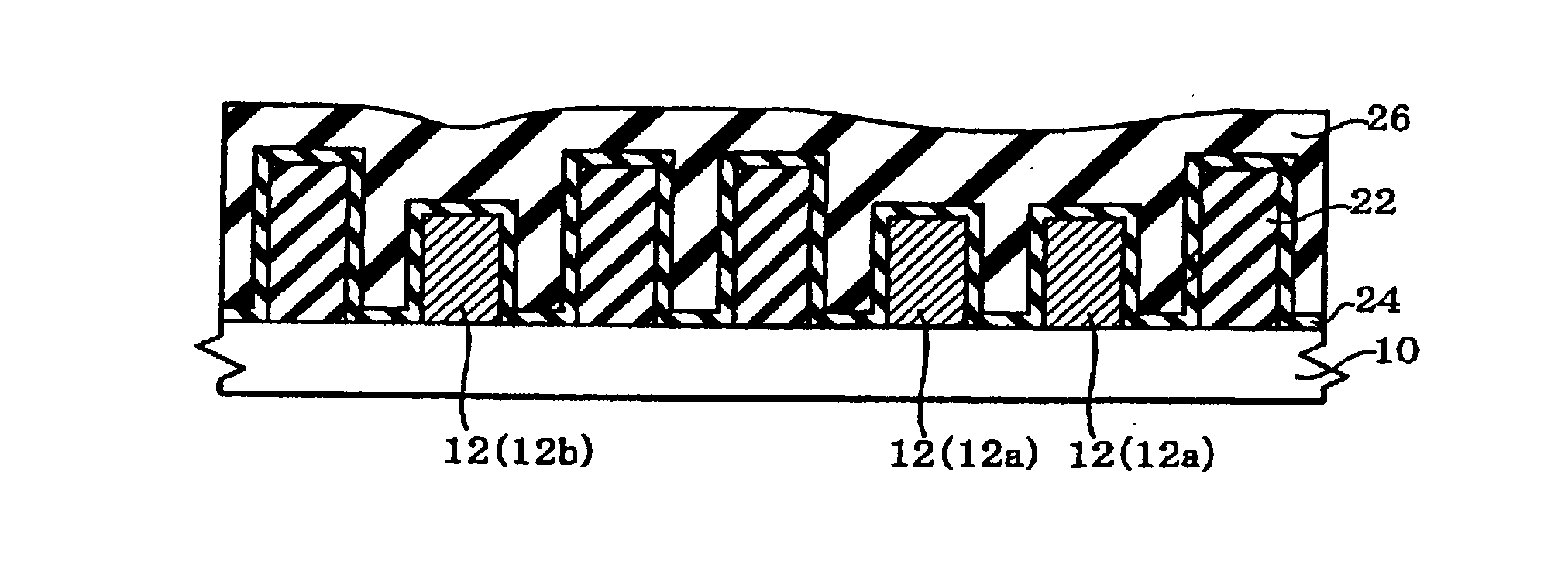
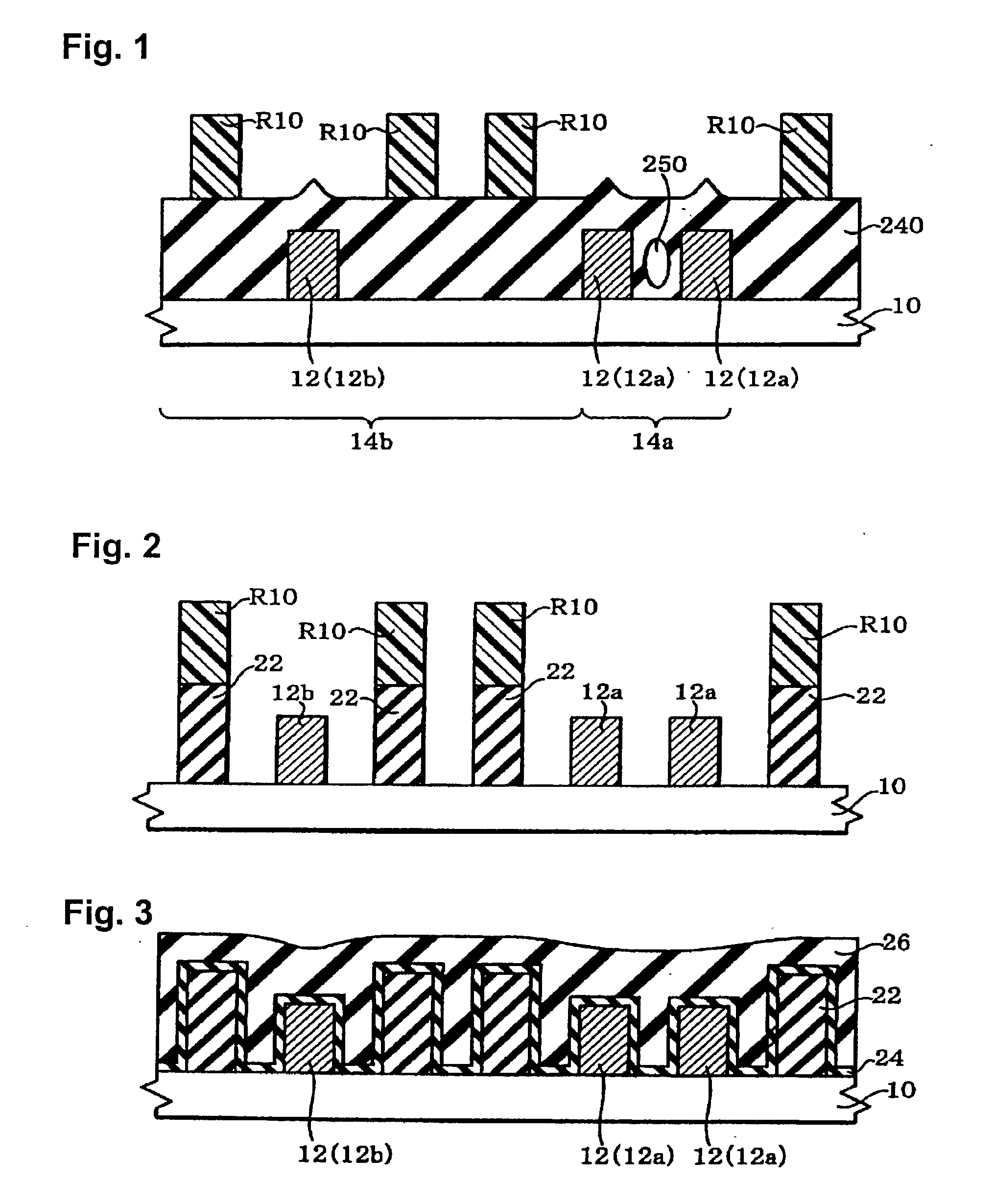
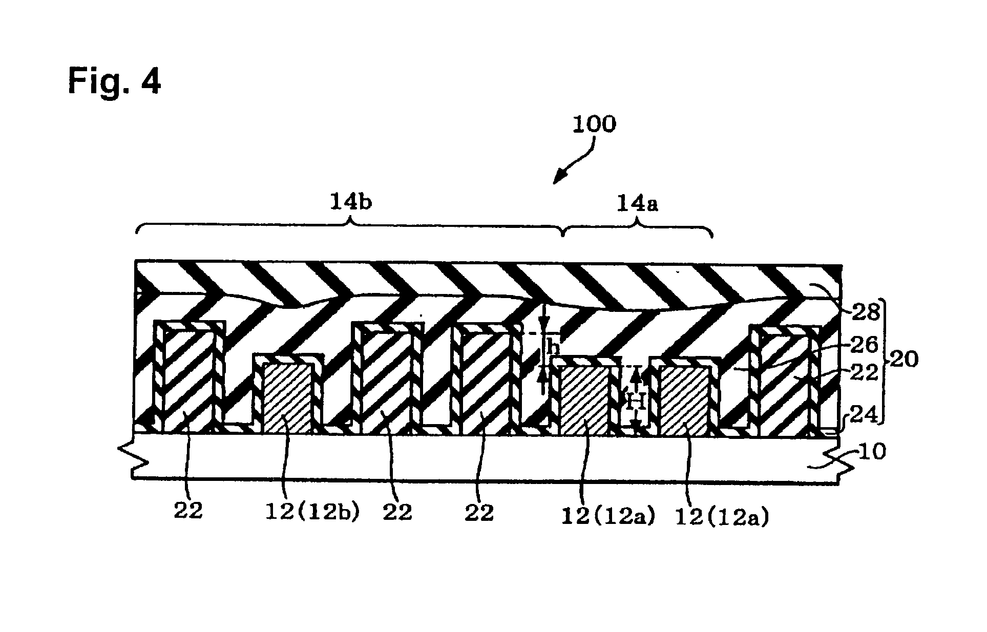
[0034] First, a semiconductor device in accordance with the present embodiment will be described. FIG. 4 schematically shows a cross-sectional view of a main part of a semiconductor device 100 of the present embodiment, and FIG. 5 schematically shows a plan view of a part of the layers of the semiconductor device 100.
[0035] The semiconductor device 100 includes a base 10, wiring layers 12 (12a, 12b) formed on the base 10, and an interlayer dielectric layer 20 that is formed in a manner to cover the wiring layers 12. Here, the "base" indicates a structural body below one interlayer dielectric layer 20. For example, when the interlayer dielectric layer 20 is an interlayer dielectric layer in the second layer, the base 10 may be formed, although not shown, from a semiconductor substrate, and an element isolation region, a semiconductor element such...
PUM
| Property | Measurement | Unit |
|---|---|---|
| width | aaaaa | aaaaa |
| width | aaaaa | aaaaa |
| width | aaaaa | aaaaa |
Abstract
Description
Claims
Application Information