Dry etch release of MEMS structures

a technology of mems and etching, which is applied in the direction of microstructural technology, microstructural devices, microstructure devices, etc., can solve the problems of stiction, no. 1 yield limit problem, and the deformation of the membrane or diaphragm from its intended position,

Inactive Publication Date: 2003-05-01
APPLIED MATERIALS INC
View PDF0 Cites 42 Cited by
  • Summary
  • Abstract
  • Description
  • Claims
  • Application Information

AI Technical Summary

Problems solved by technology

Surface micromachining fabrication processes for the electrostatic comb driver, as well as other beams and lever arms, have problems with stiction of such beams and lever arms to an underlying layer over which the beam or arm extends.
In the case of a membrane or diaphragm, the membrane or diaphragm becomes deformed from its intended position and may become stuck to an adjacent surface.
Stiction is the number one yield limiting problem in the production of the kinds of devices described above.
The authors describe how one of the major issues in surface micromachining is process-induced stiction of highly compliant microstructures to an underlying layer.
The supercritical dry method is said to generate excellent results, but this method requires the use of high pressure equipment which is not desirable in a fabrication process, due to equipment cost and safety issues.
Applicants' review of the background art in general has indicated that stiction is the primary cause of low yield in the fabrication of MEMS devices.
Factors which may contribute to stiction include: warpage due to residual stresses induced from materials; liquid-to-solid surface tension which induces collapse; drying conditions during processing; adverse and harsh forces from wet baths; aggressive designs (i.e. long and thin beams); surface-to surface attractions; inadequate cleaning techniques; aggressive cleaning techniques; and environments subsequent to fabrication, including packaging, handling, transportation, and device operation.
However, in some instances stiction occurs during the release process and prior to application of a stiction-preventing coating.
In some instances, the surface properties of the structure surfaces which were in contact with the sacrificial layer, and which remain after removal of the sacrificial layer, are not as desired after the final cycle.

Method used


Image

  • Dry etch release of MEMS structures
  • Dry etch release of MEMS structures
  • Dry etch release of MEMS structures

Examples


example one

Removal of a Silicon Oxide Sacrificial Layer

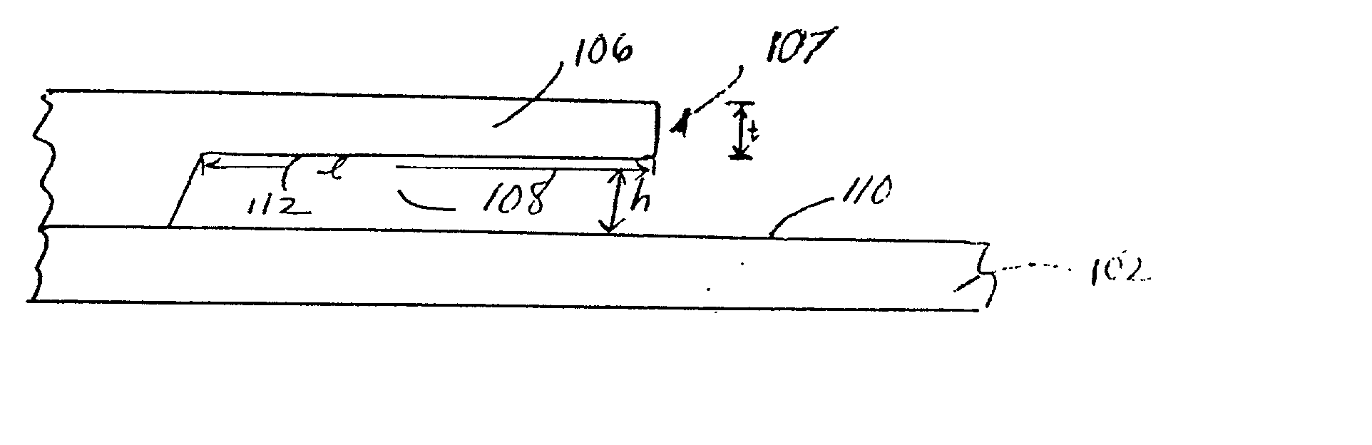
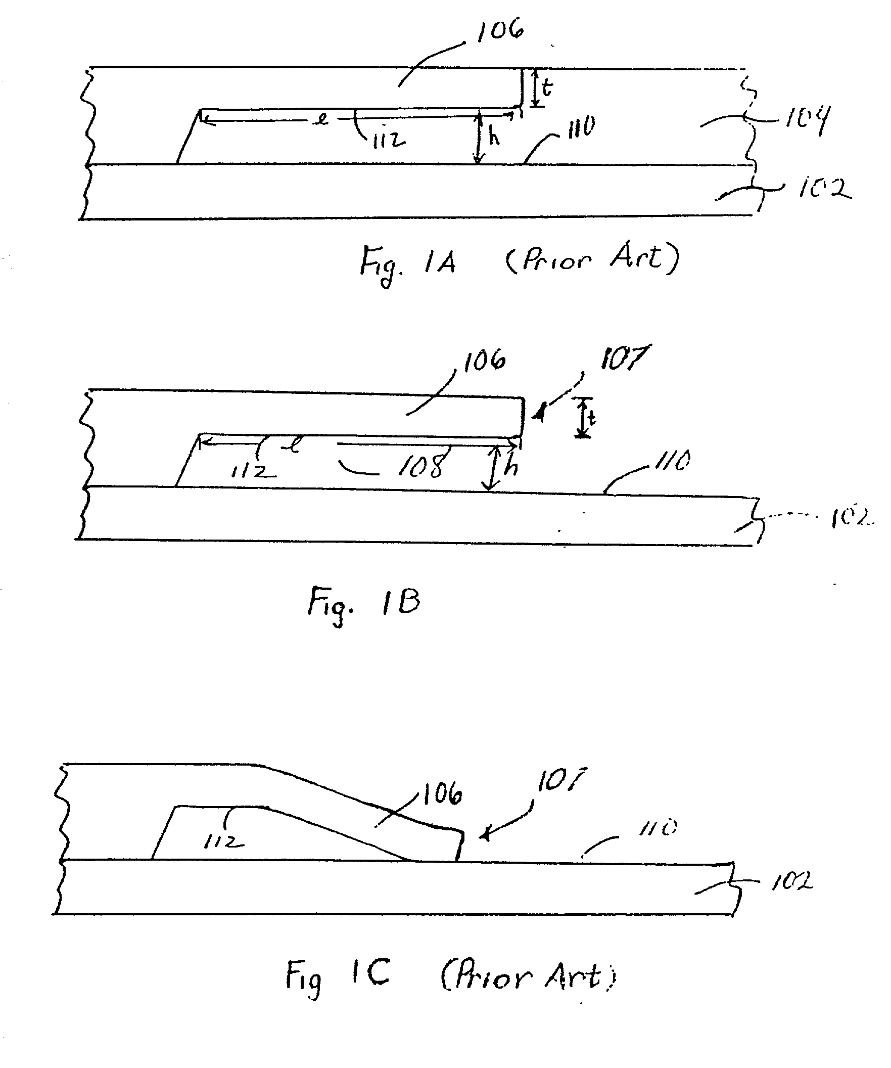
[0028] In one embodiment of the present invention a micromachined polysilicon actuator is fabricated. During fabrication of the actuator, a starting structure of the kind illustrated in FIG. 1A is used to generate a lever arm 107 of the kind shown in FIG. 1B. The actuator includes an actuation electrical contact pad (not shown). With respect to the FIG. 1A starting structure, a first portion of the upper surface 110 of a silicon substrate 102 is in contact with an overlying layer of silicon oxide 104, while a second portion of the upper surface 110 is in contact with a layer 106 of polysilicon. A portion of the bottom surface 112 of polysilicon layer 106 is also in contact with silicon oxide layer 104, in the area where silicon oxide layer 104 overlies silicon substrate 102, so that polysilicon layer 106 extends over the upper surface 110 of silicon substrate 102. Silicon oxide layer 104 then fills a gap having a height "h", between the up...

example two

Application of a SAM

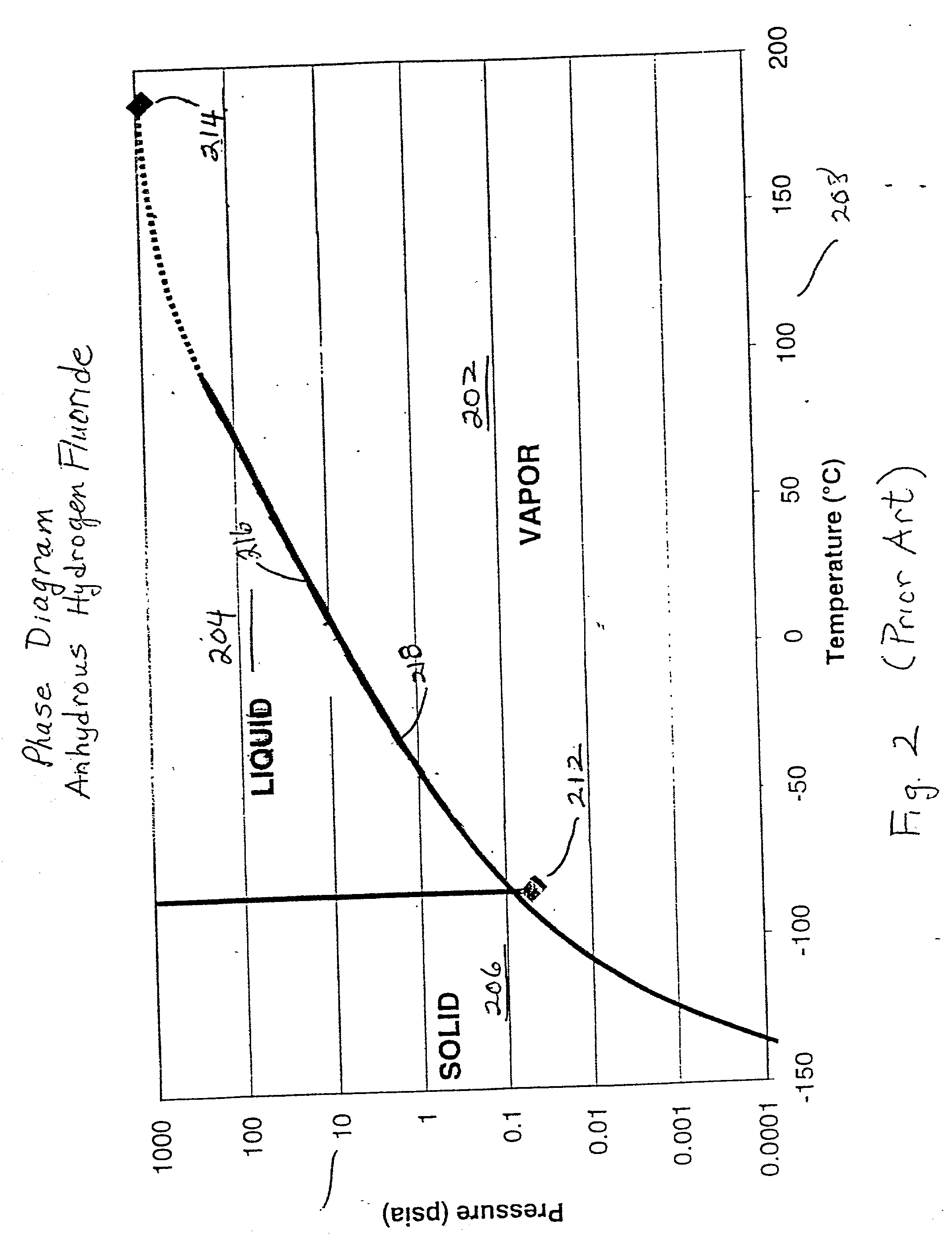
[0042] Depending on the device and the end-use application, it may be desirable to use a subsequent surface passivation treatment, such as an ammonium fluoride treatment and / or to apply a coating over the substrate which will prevent stiction during handling and use of the device. Self Assembling Monolayer (SAM) coatings are known in the art. One of the more advantageous SAMs is the coating described in U.S. Pat. No. 5,403,665, the subject matter of which is hereby incorporated by reference in its entirety. In particular, the exposed polysilicon, silicon, or silicon nitride surfaces are exposed to an oxidant. Oxidation methods known to those skilled in the art are applicable, and may be carried out in the same process chamber as that used for the etch / clean cycle steps. After exposure to an oxidant, the exposed surfaces are contacted with vapor-phase alkylsilane-containing molecules. Alkylhalosilane reagents such as alkylchlorosilane perform particularly well. Sp...


PUM

PropertyMeasurementUnit
volume %aaaaaaaaaa
temperatureaaaaaaaaaa

Abstract

The present invention pertains to a method of fabricating a surface within a MEM which is free moving in response to stimulation. The free moving surface is fabricated in a series of steps which includes a release method, where release is accomplished by a plasmaless etching of a sacrificial layer material. An etch step is followed by a cleaning step in which by-products from the etch step are removed along with other contaminants which may lead to stiction. There are a series of etch and then clean steps so that a number of "cycles" of these steps are performed. Between each etch step and each clean step, the process chamber pressure is typically abruptly lowered, to create turbulence and aid in the removal of particulates which are evacuated from the structure surface and the process chamber by the pumping action during lowering of the chamber pressure. The final etch / clean cycle may be followed by a surface passivation step in which cleaned surfaces are passivated and / or coated.

Description

[0001] In general, the present invention relates to a method of dry, plasmaless etch of MEMS (micro-electro-mechanical systems) structures, which includes a release step in which gaps are opened (etched) between various structural surfaces. For example, surface machined cantilever beams and lever arms may be fabricated by etching away sacrificial layers within a structure; or, thin membranes or diaphragms for sensors or pumps may be created by hollowing out areas of a structure.BRIEF DESCRIPTION OF THE BACKGROUND ART[0002] Micromachining technology compatible with semiconductor processes is used to produce a number of devices such as piezoelectric motors containing cantilever beams, hinges, accelerometers, reflector antennae, microsensors, microactuators, and micromirrors, for example. One of the most popular microactuators is an electrostatic comb driver, due to its simplicity in fabrication and low power consumption. Surface micromachining fabrication processes for the electrostat...

Claims


Application Information

Patent Timeline
Patent Type & Authority Applications(United States)
IPC IPC(8): B81B3/00
CPCB81B3/0005B81B3/0008B81C2201/112B81C2201/016B81B2201/033B81C1/00936
Inventor CHINN, JEFFREY D.GOPAL, VIDYUTSOUKANE, SOFIANEBECKY LEUNG, TOI YUE
Owner APPLIED MATERIALS INC
Why Eureka
Try Eureka