

Semiconductor device and method for manufacture thereof
a technology of semiconductor devices and insulating films, which is applied in the direction of semiconductor devices, basic electric elements, electrical appliances, etc., can solve the problems of reducing the effective dielectric constant of the entire gate insulating film, and the inability to enhance the performance of the mosfet, so as to prevent the increase of the gate leakage current and small leakage current
- Summary
- Abstract
- Description
- Claims
- Application Information
AI Technical Summary
Benefits of technology
Problems solved by technology
Method used
Image

Examples
first embodiment
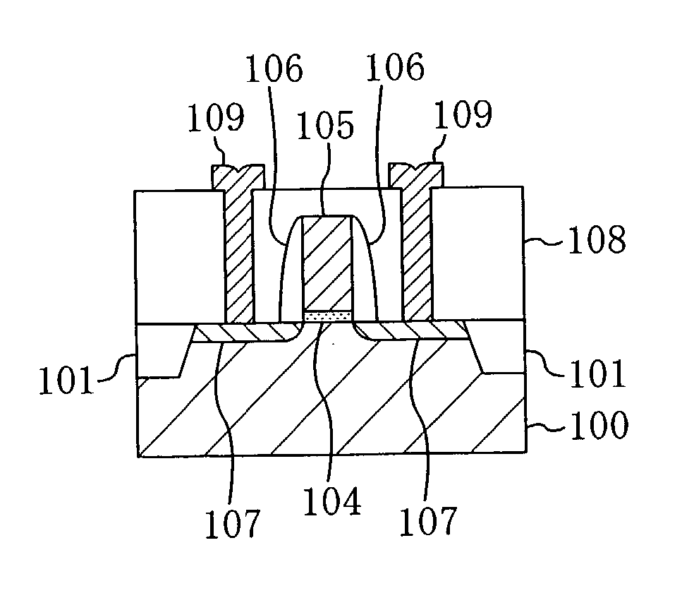
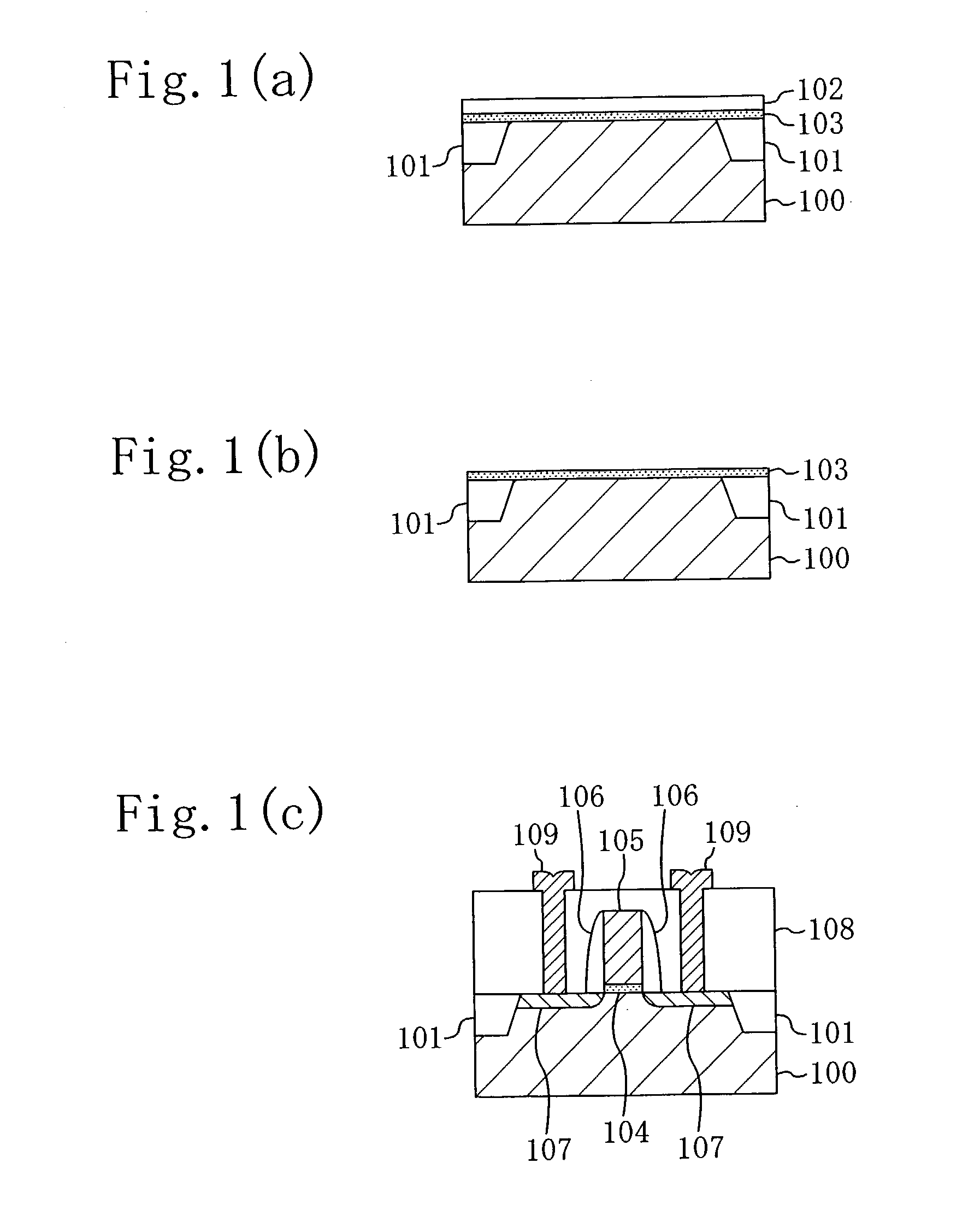
[0065] Hereafter, taking an n-type MOSFET as an example, a method for fabricating a semiconductor device in accordance with a modified example of the present invention will be described.
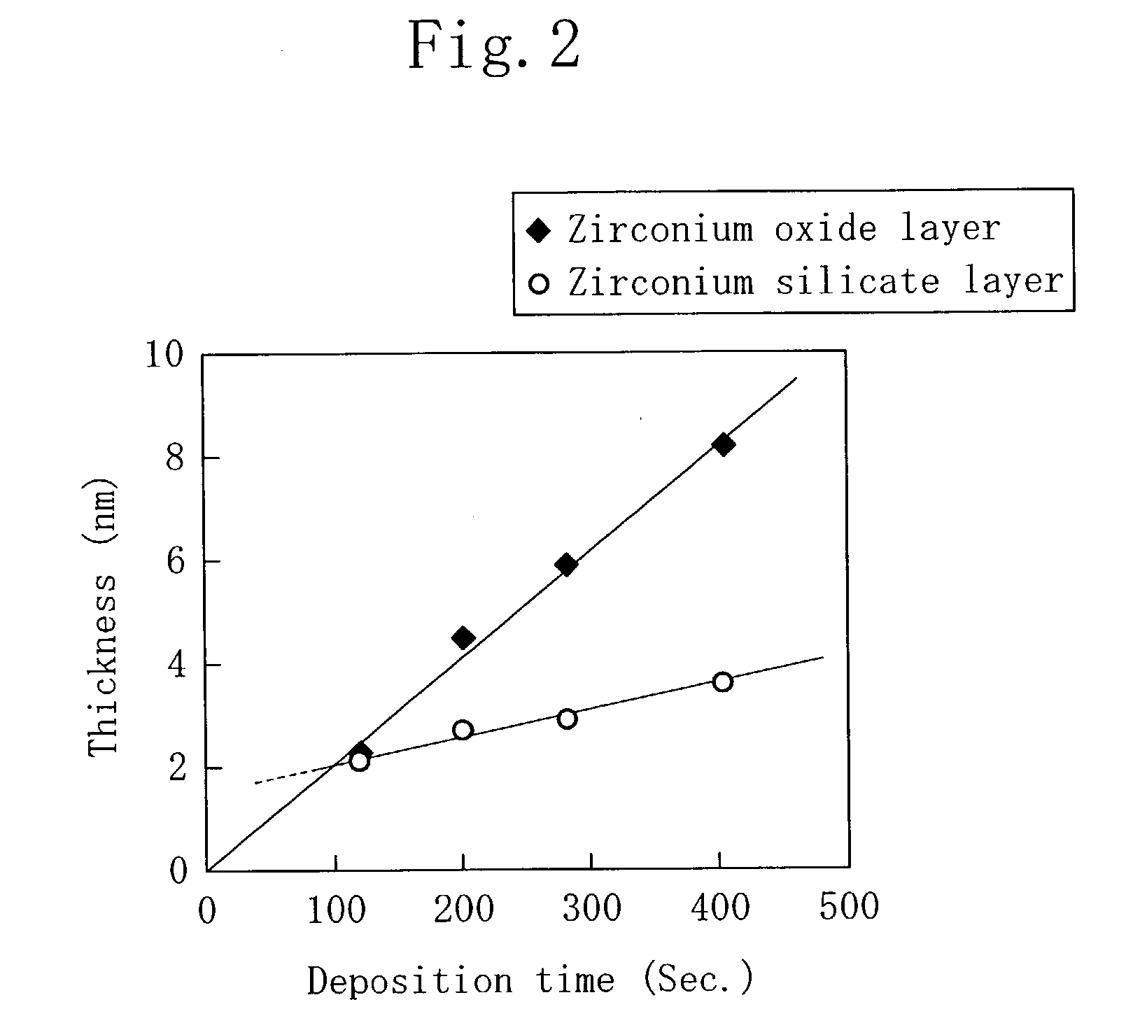
[0066] The modified example of the first embodiment is different from the first embodiment in that a chemical vapor deposition method, instead of the reactive sputtering method, is used to form a zirconium silicate layer 103 and a zirconium oxide layer 102 in the process step shown in FIG. 1(a).
[0067] Specifically, after an isolation 101 is formed, an oxide film (silicon oxide layer) having a thickness of about 1 nm is formed on the surface of a silicon substrate 100 in an H.sub.2O ambient at high temperature, in the initial stage of a chemical vapor deposition process. Then, a zirconium oxide layer 102 is formed over the silicon substrate 100 by a chemical vapor deposition method using a gaseous mixture of H.sub.2O and ZrCl.sub.4 as a source gas. In this process step, a reaction occurs between the s...
second embodiment
[0073] Second Embodiment
[0074] Hereafter, taking an n-type MOSFET as an example, a semiconductor device in accordance with a second embodiment of the present invention and a method for fabricating the same will be described with reference to the accompanying drawings.
[0075] FIGS. 3(a) and 3(b) are cross-sectional views illustrating process steps of a method for fabricating the semiconductor device in the second embodiment.
[0076] The semiconductor device fabrication method in the second embodiment is characterized as follows: a metal silicate layer is formed on a silicon substrate, a metal oxide layer is also formed on the metal silicate layer, the metal oxide layer is then removed, and thereafter another metal oxide layer is formed, thereby forming a gate insulating film made of the metal silicate layer and said another metal oxide layer. In the second embodiment, until the process step shown in FIG. 1(b), the same process steps as in the first embodiment or the modified example the...
third embodiment
[0086] Third Embodiment
[0087] Hereafter, taking an n-type MOSFET as an example, a semiconductor device in accordance with a third embodiment of the present invention and a method for fabricating the same will be described with reference to the accompanying drawings.
[0088] FIGS. 4(a) through 4(e) are cross-sectional views illustrating process steps of a method for fabricating the semiconductor device in the third embodiment.
[0089] The semiconductor device fabrication method in the third embodiment is characterized as follows: a metal silicate layer is formed on a silicon substrate, a metal oxide layer is also formed on the metal silicate layer, and the metal oxide layer is then partially removed, thereby forming a first gate insulating film made of the metal silicate layer, and a second gate insulating film made of the metal silicate layer and the metal oxide layer. In the third embodiment, a reactive sputtering method, for example, is used to form the metal silicate layer and the me...
PUM
| Property | Measurement | Unit |
|---|---|---|
| thickness | aaaaa | aaaaa |
| dielectric constant | aaaaa | aaaaa |
| thickness | aaaaa | aaaaa |
Abstract
Description
Claims
Application Information