Field emission photo-cathode array for lithography system and lithography system provided with such an array

a technology of lithography system and array, which is applied in the field of field emission photocathode array for lithography system and lithography system provided with such array, can solve the problems of wasting a long time to write a whole wafer with this single beam, and not being able to achieve sharpening up or resolution enhancement,

Inactive Publication Date: 2003-09-25
ASML NETHERLANDS BV
View PDF6 Cites 28 Cited by
  • Summary
  • Abstract
  • Description
  • Claims
  • Application Information

AI Technical Summary

Benefits of technology

0048] FIGS. 10a and 10b show holes in the semiconductor layer to prevent cross talk between adjacent electron sources.

Problems solved by technology

The sharpening up, or enhancement of resolution, cannot be done after the mixing of information has occurred.
However, it would take a long time to write a whole wafer with this single beam.
However, by that time it was thought that this could only be achieved by providing for each field emitter individual control by light switches on which the light beamlets impinge.

Method used


Image

  • Field emission photo-cathode array for lithography system and lithography system provided with such an array
  • Field emission photo-cathode array for lithography system and lithography system provided with such an array
  • Field emission photo-cathode array for lithography system and lithography system provided with such an array

Examples


Embodiment Construction

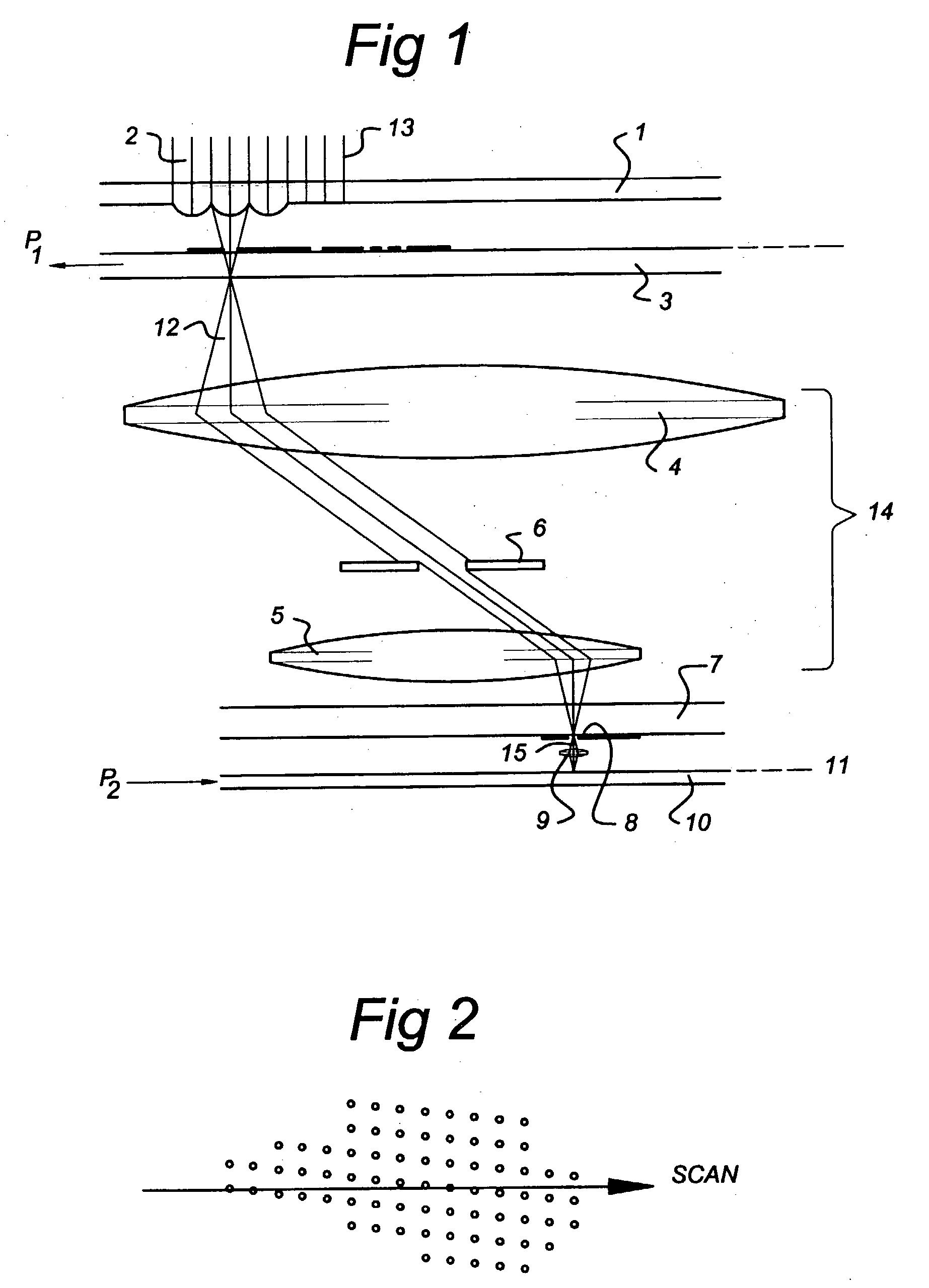
[0051] FIGS. 1 and 2 have been explained above.

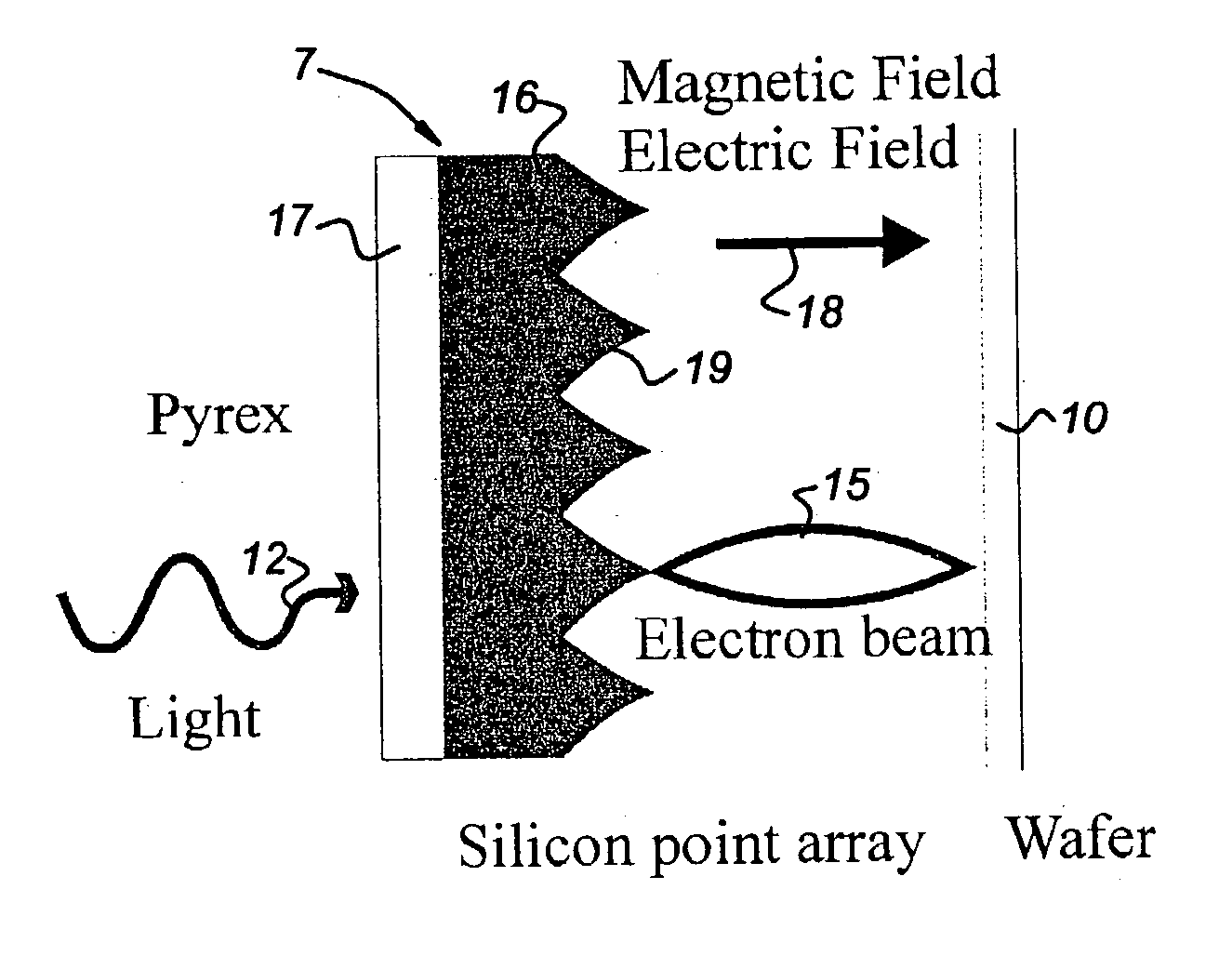
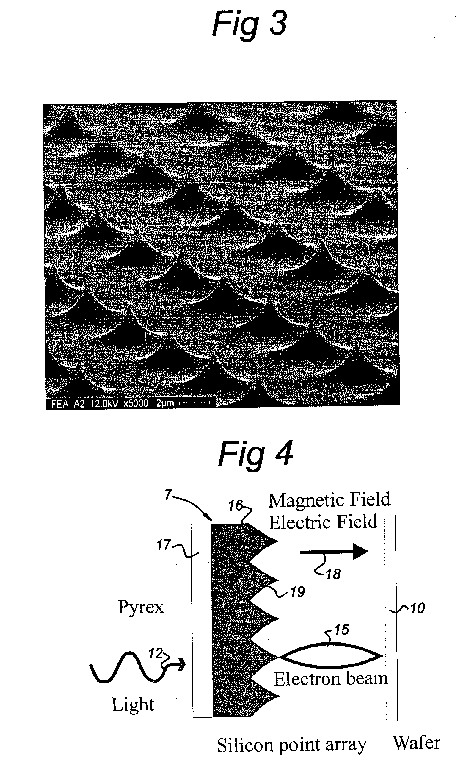
[0052] In accordance with the invention the converter plate 7 comprises a semiconductor field emission array as shown in FIG. 3. FIG. 3 shows a plurality of tips on a p-doped silicon substrate. The image has been made by means of a Scanning Electron Microscope (SEM). The silicon wafer was sized 5 mm.times.5 mm. 81.times.81 tips were etched on the wafer surface. The tips shown were spaced about 8 .mu.m whereas their height was about 4 .mu.m. Of course, these figures are only examples. To further enhance the resolution on the wafer 10 to be processed, it is envisaged that the tips may be located closer to one another than 8 .mu.m.

[0053] The front surface from the tips, from which the electrons leave the silicon, have a diameter of preferably less than 100 nm, even more preferably less than 50 nm.

[0054] FIG. 3 shows conically shaped tips. However, the invention is not limited to such a shape. The tips may have a rectangle or other shaped c...


PUM

PropertyMeasurementUnit
diameteraaaaaaaaaa
diameteraaaaaaaaaa
heightsaaaaaaaaaa

Abstract

The present invention relates to the use of an electron source in a lithography system for producing a plurality of electron beams directed towards an object to be processed, said electron source comprising a plurality of field emitters, characterized in that said electron source comprises a semiconductor layer with a plurality of tips, said use including the steps of: producing a plurality of light spots on said electron source, producing one light spot on one field emitter; exciting electrons to a conduction band (Ec) by light from a light spot within said field emitter by a photo-electric effect; accelerating said electrons in said conduction band (Ec) towards said tips and tunnelling them outside tips in order to generate electrons for said plurality of electron beams, causing tips to generate electrons for said electron beam having a spot smaller than 100 nm on an object to be processed, each spot of light triggering an electron beam from one tip.

Description

[0001] The invention relates to using an electron source for producing at least one electron beam directed towards and focused on an object to be processed, the electron source comprising at least one field emitter.[0002] The invention also relates to a lithography system provided with such a converter element.PRIOR ART[0003] Converter elements for use in lithography systems, and designed to convert a light beam into a beam of charged particles are known from W098 / 54620. The purpose of these converter elements is to provide a better resolution (0.1 .mu.m or less) in such systems than was possible with prior art systems without such converters in which the resolution was entirely determined by the wavelength of the light beam used.[0004] First of all a description of such a system as described in W098 / 54620 is given.[0005] To that end, reference is made to FIG. 1.[0006] The background of the system described in W098 / 54620 is as follows.[0007] Imagine that there is provided a known de...

Claims


Application Information

Patent Timeline
Patent Type & Authority Applications(United States)
IPC IPC(8): G03F7/20H01J1/304H01J1/34H01J37/073H01J37/317
CPCB82Y10/00B82Y40/00G03F7/70375H01J1/304H01J2237/31779H01J37/073H01J37/3175H01J2201/317H01J2237/06333H01J1/34
Inventor KAMPHERBEEK, BERT JANWIELAND, MARCO JAN-JACOKRUIT, PIETER
Owner ASML NETHERLANDS BV
Why Eureka
Try Eureka