Nitride semiconductor, method for manufacturing the same and nitride semiconductor device

a technology of nitride semiconductor and semiconductor device, which is applied in the direction of semiconductor lasers, lasers, solid-state devices, etc., can solve the problems of cracks and defects, large lattice distortion, and difficult to obtain laser structure without cracks

Inactive Publication Date: 2003-10-02
PANASONIC CORP
View PDF3 Cites 96 Cited by
  • Summary
  • Abstract
  • Description
  • Claims
  • Application Information

AI Technical Summary

Problems solved by technology

On the other hand, when a semiconductor layer made of AlGaN with smaller bulk lattice coefficient than GaN is grown on a GaN layer grown on a substrate made of gallium nitride (GaN), i.e., on the cognate substrate, as well known, the larger an Al composition becomes, the larger a lattice distortion becomes and cracks and defects are increased.
Thus, it is difficult to obtain a laser structure without cracks being generated.

Method used


Image

  • Nitride semiconductor, method for manufacturing the same and nitride semiconductor device
  • Nitride semiconductor, method for manufacturing the same and nitride semiconductor device
  • Nitride semiconductor, method for manufacturing the same and nitride semiconductor device

Examples


first embodiment

[0100] A modified example of the present invention will be described hereinafter with reference to the drawings.

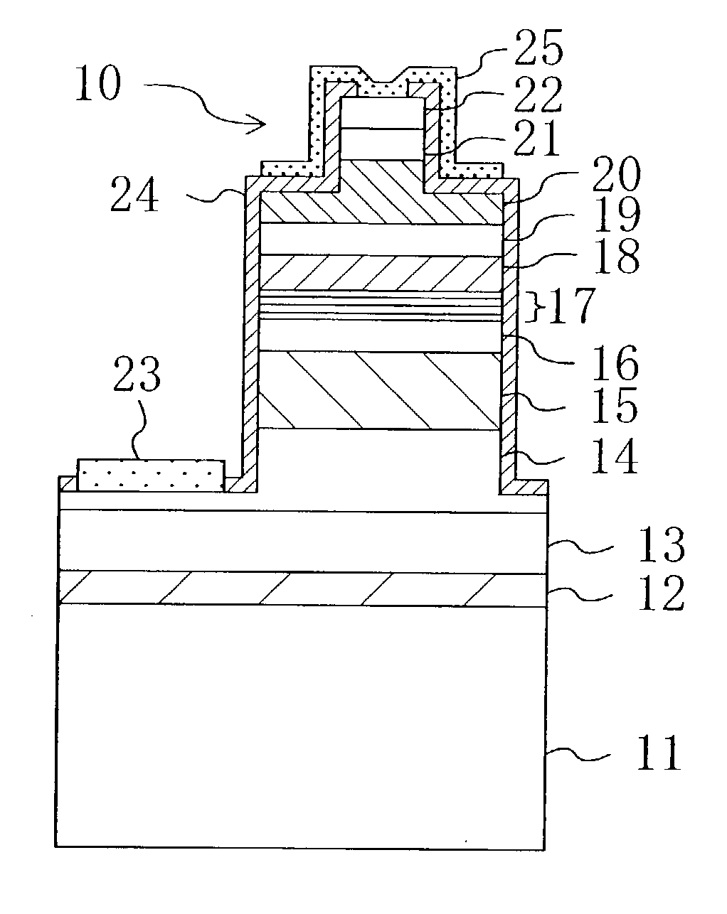
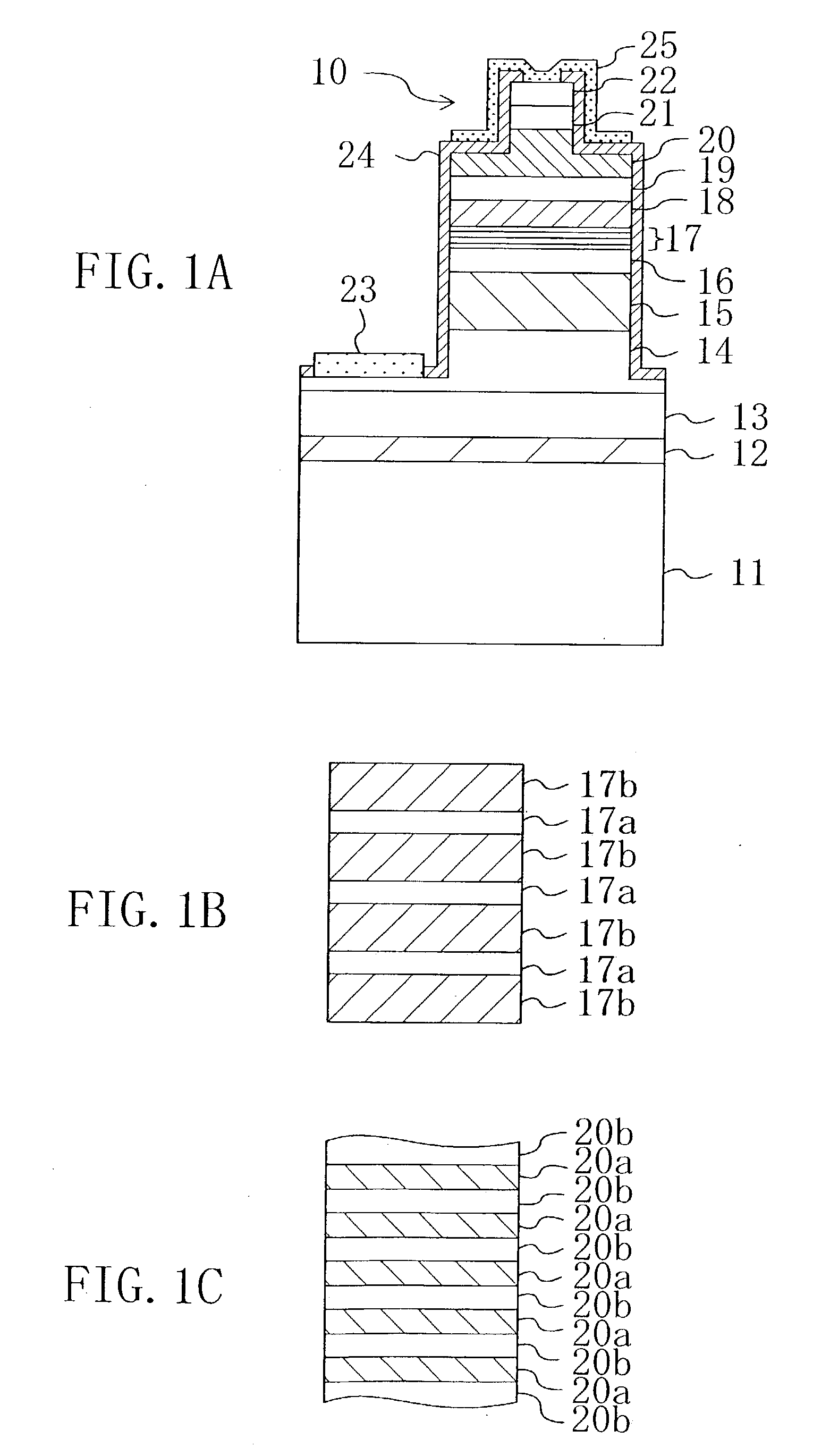
[0101] FIG. 4 shows a cross-sectional structure of nitride semiconductor laser device relating to a modified example of the first embodiment of the present invention. Referring to FIG. 4, the same structural members as those of FIG. 1(a) are denoted by the same reference numerals and description thereof will be omitted.

[0102] As shown in FIG. 4, in accordance with this modified example, instead of the substrate 11 made of undoped gallium nitride (GaN), an n-type conductive substrate 31 made of n-type gallium nitride into which an n-type dopant such as silicon (Si), germanium (Ge) or oxygen (O) is added is used.

[0103] In accordance with a method for manufacturing the semiconductor laser device of this modified example, an n-type facet-forming layer 32 made of n-type AlGaInN with Si or the like being added thereto is formed on the n-type substrate 31. On the formed n-type fa...

second embodiment

[0108] Second Embodiment

[0109] A second embodiment of the present invention will be described hereinafter with reference to the drawings.

[0110] FIG. 5 shows a cross-sectional structure of nitride semiconductor laser device relating to a second embodiment of the present invention. Referring to FIG. 5, the same structural members as those of FIG. 1(a) are denoted by the same reference numerals and descriptions thereof will be omitted.

[0111] As shown in FIG. 5, in accordance with a semiconductor laser device relating to the second embodiment, a selective growth layer 41 that is made of AlGaInN and has a plurality of recessed portions 41a extending in a stripe manner is formed by growth on the facet-forming layer 12 made of AlGaInN. A mask film 42 made of, e.g., silicon nitride (SiN.sub.x) is formed on a bottom surface and a wall surface of each recessed portion 41a of the selective growth layer 41.

[0112] A lateral growth layer 43 made of GaN is formed by growth on a surface of the sele...

first modified example

[0121] First Modified Example of Second Embodiment

[0122] A first modified example of the second embodiment of the present invention will be described hereinafter with reference to the drawings.

[0123] FIG. 7 shows a cross-sectional structure of nitride semiconductor laser device relating to the first modified example of the second embodiment of the present invention. Referring to FIG. 7, the same structural members as those of FIG. 5 are denoted by the same reference numerals and descriptions thereof will be omitted.

[0124] As shown in FIG. 7, in accordance with the first modified example, instead of the substrate 11 made of undoped GaN, a conductive n-type substrate 31 made of n-type gallium nitride into which an n-type dopant such as Si, Ge or O is added is used.

[0125] In accordance with a method for manufacturing the semiconductor laser device of the first modified example, on the n-type substrate 31, an n-type facet-forming layer 32 made of n-type AlGaInN with Si or the like being...


PUM

PropertyMeasurementUnit
oscillation wavelengthaaaaaaaaaa
thicknessaaaaaaaaaa
thicknessaaaaaaaaaa

Abstract

A facet-forming layer made of nitride semiconductor containing at least aluminum is formed on a substrate made of gallium nitride (GaN). A facet surface inclined with respect to a C-surface is formed on the surface of the facet-forming layer, and a selective growth layer laterally grows from the inclined facet surface. As a result, the selective growth layer can substantially lattice-match an n-type cladding layer made of n-type AlGaN and grown on the selective growth layer. For example, a laser structure without cracks being generated can be obtained by crystal growth.

Description

[0001] This application is continuation of Application PCT / JP02 / 05929, filed Jun. 13, 2002, now abandoned.[0002] The present invention relates to a nitride semiconductor and a method for manufacturing the same, and in particular, to a nitride semiconductor device that is formed by the manufacturing method and expected to be applied to a field of optical information processing.[0003] A nitride semiconductor containing nitrogen (N) as an element of the group V is considered to be hopeful as materials for short wavelength luminous element because its band gap is relatively large. Among the nitride semiconductors, a gallium nitride-based compound semiconductor that is represented by general formula Al.sub.xGa.sub.yIn.sub.zN (wherein 0.ltoreq.x, y, z.ltoreq.1, x+y+z=1) has been studied hard Blue light emitting diode (LED) device and green light emitting diode device have already been in practical use.[0004] A short wavelength semiconductor laser device with about 400 nm of oscillation wa...

Claims


Application Information

Patent Timeline
Patent Type & Authority Applications(United States)
IPC IPC(8): H01L21/20H01L33/00H01S5/343
CPCB82Y20/00H01L33/007H01S5/34333H01L21/0237H01L21/02458H01L21/0265H01L21/0254H01L21/02576H01L21/0262H01L21/02639H01L21/02505
Inventor KAWAGUCHI, YASUTOSHIISHIBASHI, AKIHIKOTSUJIMURA, AYUMUOTSUKA, NOBUYUKI
Owner PANASONIC CORP
Why Eureka
Try Eureka