Light-emitting device, liquid-crystal display device and method for manufacturing same

a technology of liquid crystal display and light-emitting device, which is applied in the direction of organic semiconductor devices, instruments, optics, etc., can solve the problems of increasing interconnection resistance, increasing power consumption, and forming of encounter projections such as whiskers

Inactive Publication Date: 2003-10-16
SEMICON ENERGY LAB CO LTD
View PDF9 Cites 64 Cited by
  • Summary
  • Abstract
  • Description
  • Claims
  • Application Information

AI Technical Summary

Problems solved by technology

Conventionally, where TFTs are fabricated by using aluminum as a TFT gate interconnection material, there encounter projections, such as hillocks or whiskers, formed by thermal process or TFT poor operation or TFT characteristic reduction due to the diffusion of aluminum atoms into the ...

Method used


Image

  • Light-emitting device, liquid-crystal display device and method for manufacturing same
  • Light-emitting device, liquid-crystal display device and method for manufacturing same
  • Light-emitting device, liquid-crystal display device and method for manufacturing same

Examples


example [ 1

Example [1]

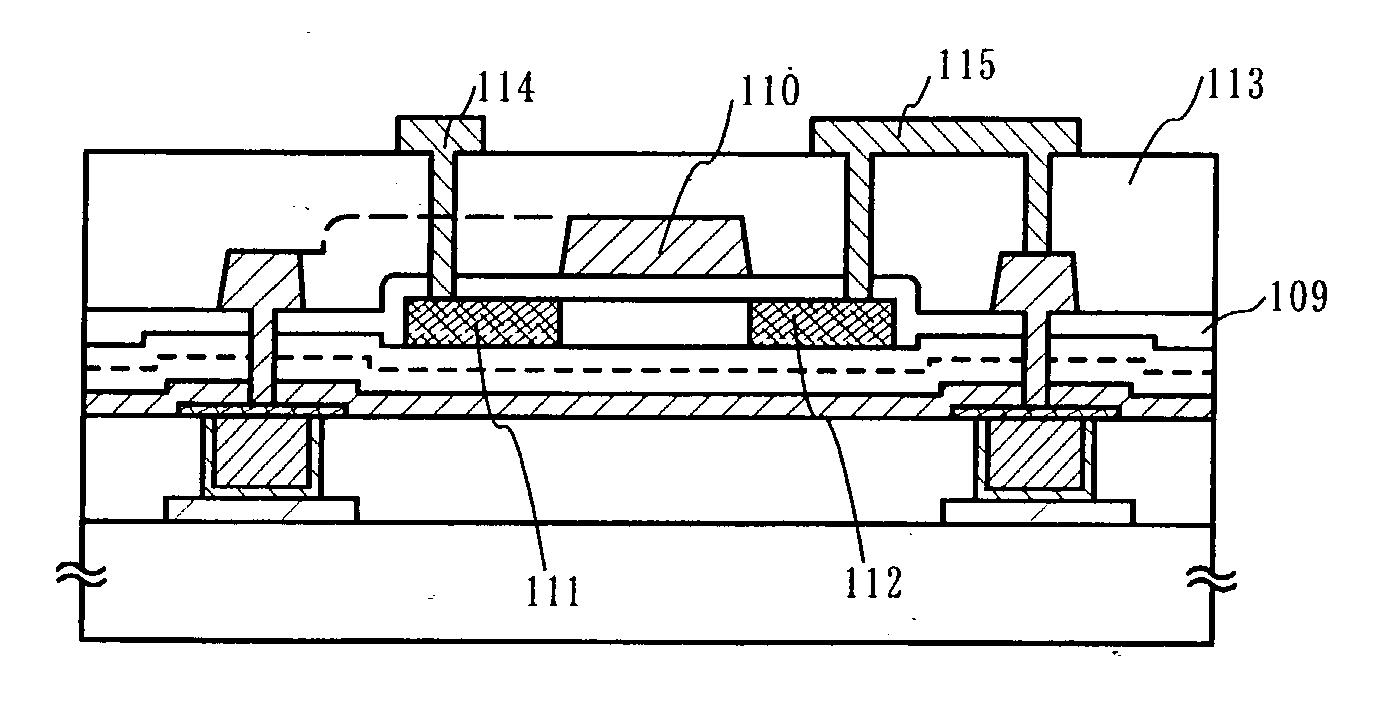
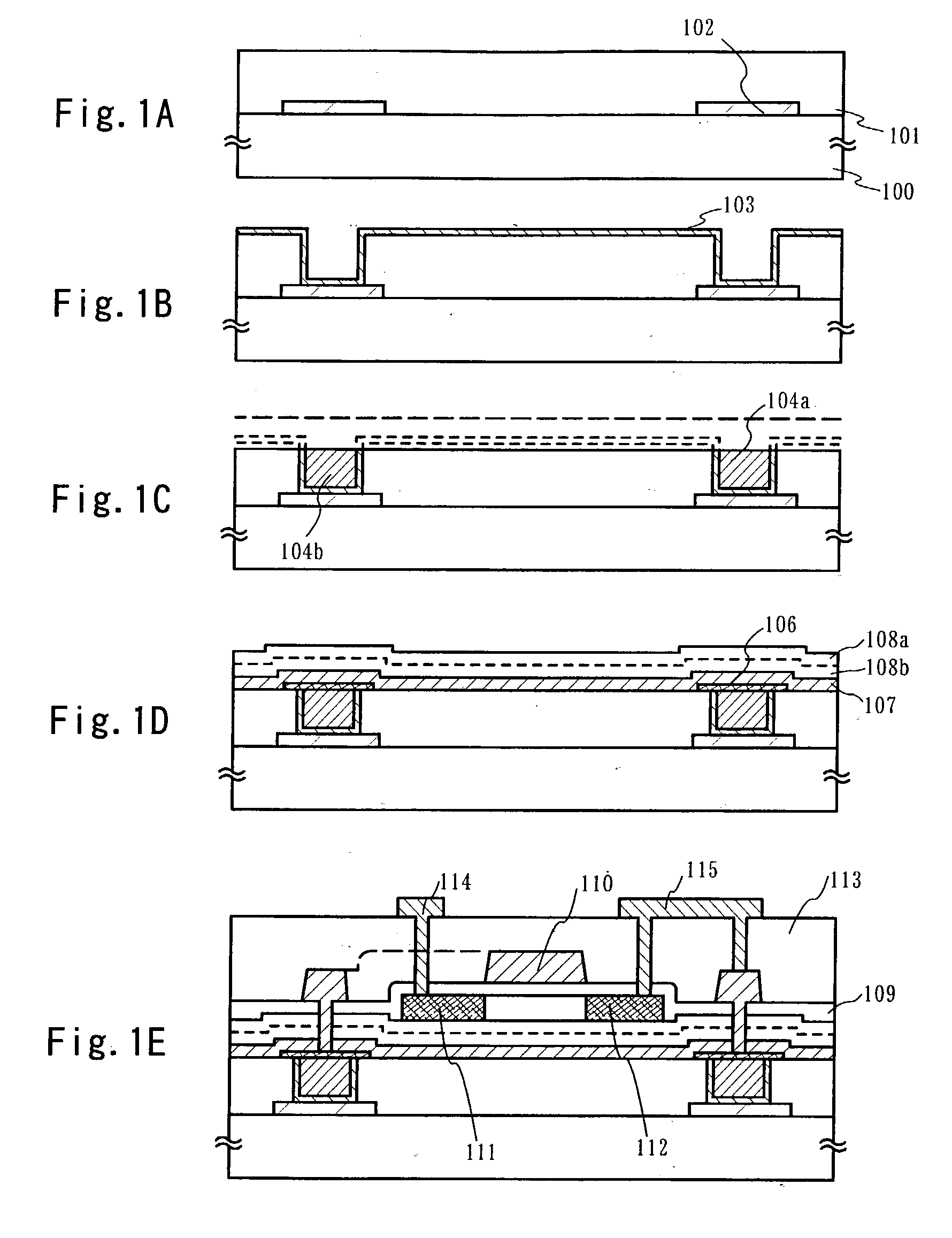
[0093] This example shows that the major part of the power supply line of a light-emitting device is made as a buried interconnection, in FIGS. 3 to 6.

[0094] At first, according to the above embodiment, an etching-stop layer is formed on a substrate having an insulating surface and a silicon-based insulating film is formed covering the etching-stop layer. The insulating film is selectively etched to form an opening (trench) reaching the etching-stop layer. After forming a first barrier layer, electrolytic plating is carried out to form a low-resistance metal film having a sufficient thickness in the opening (trench). Subsequently, planarization represented by the chemical mechanical polishing (hereinafter, referred to as CMP) is made to leave the copper and first barrier layer only in the opening (trench) but remove away unwanted portions, thereby forming an interconnection in a buried form. The top view in this process stage is shown in FIG. 3, wherein the sectional view...

example 2

[Example 2]

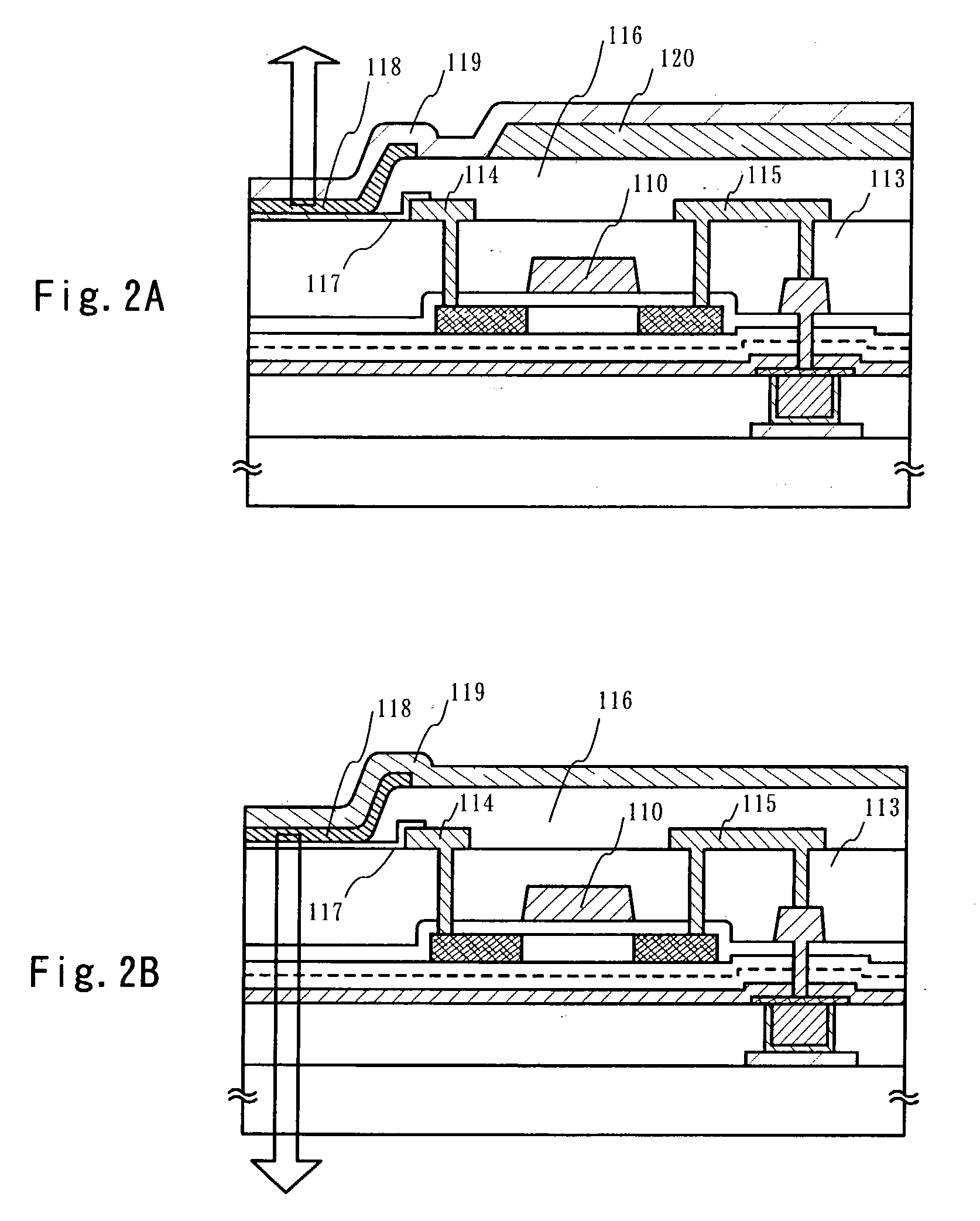
[0131] This shows an example that the major part of a gate line of a liquid-crystal display device is made by a buried interconnection, in FIGS. 12 and 13.

[0132] At first, according to the above embodiment, an etching-stop layer is formed on a substrate having an insulating surface and a silicon-based insulating film is formed covering the etching-stop layer. The insulating film is selectively etched to form an opening (trench) reaching the etching-stop layer. After forming a first barrier layer, electrolytic plating is carried out to form a low-resistance metal film having a sufficient thickness in the opening (trench). Subsequently, planarization represented by the chemical mechanical polishing (hereinafter, referred to as CMP) is made to leave the copper and first barrier layer only in the opening (trench) but remove away unwanted portions, thereby forming an interconnection in a buried form.

[0133] Then, a second barrier layer is formed in order to provide an exposed p...

example 3

[Example 3]

[0141] The drive circuit and pixel region formed by carrying out the invention can complete various modules (active-matrix liquid-crystal module, active-matrix EC module). Namely, the invention can complete an electronic apparatus built it in a display part.

[0142] Such electronic apparatuses include video cameras, digital cameras, head-mount displays (goggle type displays), car navigators, projectors, car stereo sets, personal computers, and personal digital assistants (mobile computers, cellular phones or electronic books). Examples of them are shown in FIGS. 14A to 14C and 15A and 15B.

[0143] FIG. 14A is a personal computer, including a main body 2001, an image input part 2002, a display part 2003, a keyboard 2004 and so on.

[0144] FIG. 14B is a mobile computer, including a main body 2201, a camera part 2202, an image receiving part 2203, an operation switch 2204, and a display part 2205.

[0145] FIG. 14C is a player using a recording medium recording a program (hereinafter...


PUM


Abstract

The present invention provides a structure of a semiconductor device that realizes low power consumption even where increased in screen size, and a method for manufacturing the same. The invention forms an insulating layer, forms a buried interconnection (of Cu, Au, Ag, Ni, Cr, Pd, Rh, Sn, Pb or an alloy thereof) in the insulating layer. Furthermore, after planarizing the surface of the insulating layer, a metal protection film (Ti, TiN, Ta, TaN or the like) is formed in an exposed part. By using the buried interconnection in part of various lines (gate line, source line, power supply line, common line and the like) for a light-emitting device or liquid-crystal display device, line resistance is decreased.

Description

[0001] 1. Technical Field of the Invention[0002] The present invention relates to a semiconductor device having a circuit configured with thin-film transistors (hereinafter, referred to as TFTs) and a method for manufacturing same. For example, the invention relates to an electronic apparatus mounting, as a part, an electro-optical device represented by a liquid-crystal display or a light-emitting device having OLEDs.[0003] Incidentally, the semiconductor device in this description refers to a device as a whole which is capable of functioning by the utilization of a semiconductor characteristic, i.e. electro-optical devices, semiconductor circuits and electronic apparatuses are all fallen under semiconductor devices.[0004] 2. Description of the Related Art[0005] Recently, attentions are drawn to the art to structure a thin-film transistor (TFT) by the use of a semiconductor film (thickness: approximately several to several hundred nm) formed over a substrate having an insulating sur...

Claims


Application Information

Patent Timeline
IPC IPC(8): G02F1/1362H01L21/77H01L21/84H01L27/12H01L27/32
CPCG02F1/13454G02F1/136286G02F2001/136295H01L27/124H01L27/3293H01L2251/5315H01L27/3279G02F1/136295H10K59/18H10K59/1315H10K2102/3026H05B33/00
Inventor TAKAYAMA, TORUYAMAZAKI, SHUNPEI
Owner SEMICON ENERGY LAB CO LTD
Why Eureka
Try Eureka