

Ultra fine patterning process for multi-layer substrate
a multi-layer substrate and ultra-fine technology, applied in photomechanical devices, instruments, nanoinformatics, etc., can solve problems such as time-consuming and expensive, poor reliability, and poor yield
- Summary
- Abstract
- Description
- Claims
- Application Information
AI Technical Summary
Benefits of technology
Problems solved by technology
Method used
Image

Examples
first embodiment
[0030] Please refer to FIG. 2A to FIG. 2N, which are showing the ultra fine patterning process for multi-layer substrate by using selective deposition resist of the present invention, which comprising,
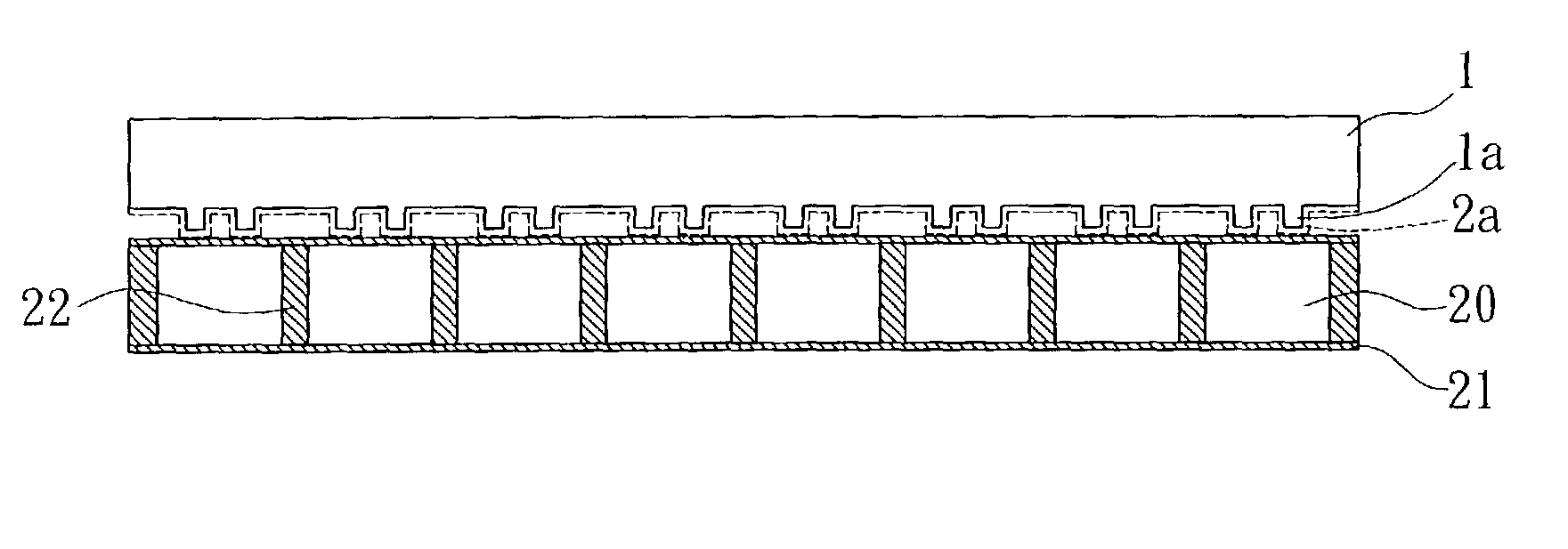
[0031] (a). providing a stamp 1 formed by a master mold, the stamp is made of elastomeric base; such as poly dimethalsiloxane (PDMS). The stamp I has been patterned with ultra fine pattern la which is corresponding to the circuit layout pattern on the substrate produced in a succeeding process; dipping the stamp 1 in a self-assembled monolayers solution 2, such as Octadecyltrichlorosilane, RsiCl3, Rsi(OCH3) etc. that are characteristic of inhibiting metal nucleation as shown in FIG. 2A.
[0032] (b). removing the stamp 1 from the self-assembled monolayers solution 2, as a result, a film characterized by metal nucleation inhibition is attached on the stamp 1, which is self-assembled monolayers (SAM) 2a as shown in FIG. 2B.
[0033] (c). providing one substrate 20, which can be a ceramic subst...
second embodiment
[0045] Please refer to FIG. 3A to FIG. 3G, which are showing the ultra fine patterning process for multi-layer substrate by using selective deposition resist of the present invention, which comprising,
[0046] (a). providing one substrate 31, which can be a ceramic substrate, a plastic substrate, a soft material substrate, a metal substrate, a glass substrate, a circuit board or a core sheet; and some stuffed vias 32 penetrating through the substrate 31 have been formed on the predetermined positions on the substrate 31; placing a dielectric layer 33 on the surface of the substrate 31, which is a photo-imagible dielectric one or a laserable layer, as shown in FIG. 3A;
[0047] (b). if the dielectric layer 33 is a photo-imagible dielectric one, the process of Exposure and Photolithography will be applied further; if the dielectric layer 33 is a laserable dielectric layer, the laser drilling will be applied to make some pattern on the dielectric layer 33 to form some circuit layout, includ...
PUM
 Abstract
Description
Claims
Application Information