Bidirectional signal transmission circuit and bus system

a transmission circuit and bus system technology, applied in the field of bidirectional signal transmission circuit and bus system, can solve the problems of data transfer rate, inconvenient operation, and difficulty in proper data transfer, and achieve the effect of fast signal transmission and facilitate impedance matching

Inactive Publication Date: 2003-10-23
PANASONIC CORP
View PDF3 Cites 21 Cited by
  • Summary
  • Abstract
  • Description
  • Claims
  • Application Information

AI Technical Summary

Benefits of technology

[0016] The second object of the invention is to provide a bus system that facilitates impedance matching and fast signal transmission.
[0017] The third object of the invention is to provide a bus interface that delivers high noise immunity in addition to the above stated effects.

Problems solved by technology

However, such speedups also incur difficulties in the proper transfer of data.
This is because disturbances such as reflections of signals due to a mismatch with a characteristic impedance of a transmission line and crosstalk between adjacent lines become more serious with increase in data transfer rate.
However, the above series termination is not applicable to a bidirectional transmission line that transmits signals in two directions, because in the case of the bidirectional transmission line its both ends will act as output ends as well as input ends.
However, when transmitting a signal from an output buffer 903, an impedance mismatch occurs due to the absence of a series terminating resistor between the output buffer 903 and the bidirectional transmission line.
However, with conventional bus interfaces, it is becoming increasingly difficult to improve clock frequencies for faster signal transmission and at the same time ensure impedance matching.
In the case of RSL in FIG. 3, when mounting an LSI (Large-Scale Integration) onto a board, leads included in the LSI package will end up being branch lines, so that it is impossible to form a bus line of single-stroke configuration which contains no branch lines.
Though such a bus line can operate without problems within a frequency range up to the order of some hundreds of megahertz, at higher frequencies (the order of gigahertz) the bus line inevitably suffers signal reflections because of the presence of several branch lines (leads) which do not match with the bus line.

Method used


Image

  • Bidirectional signal transmission circuit and bus system
  • Bidirectional signal transmission circuit and bus system
  • Bidirectional signal transmission circuit and bus system

Examples


first embodiment

[0074] First Embodiment

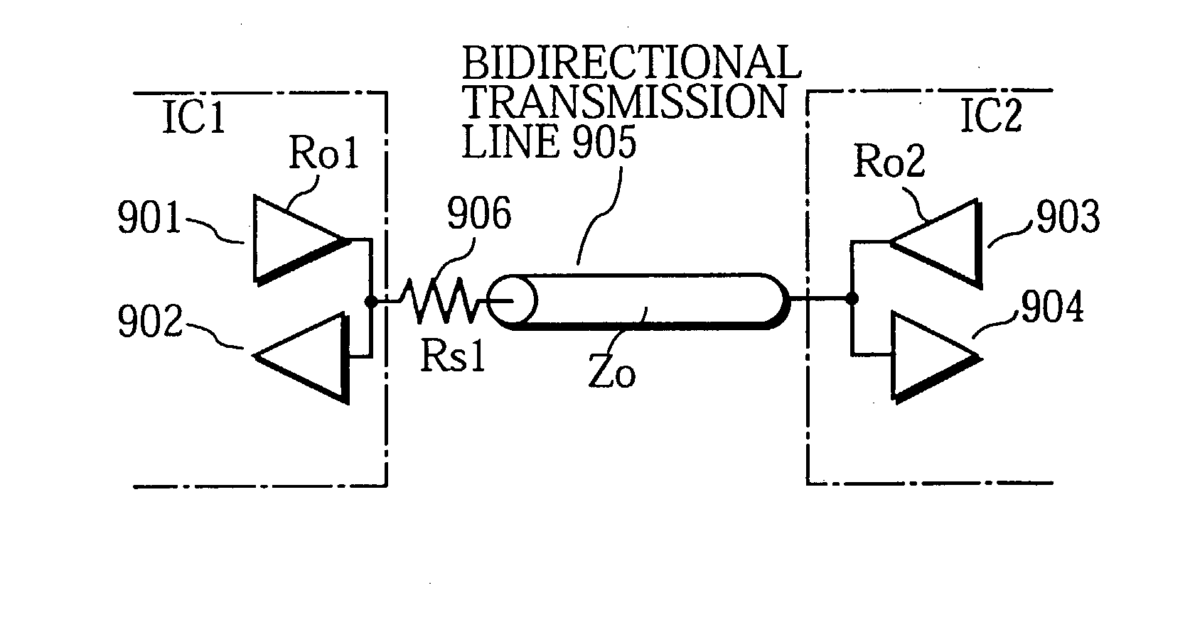
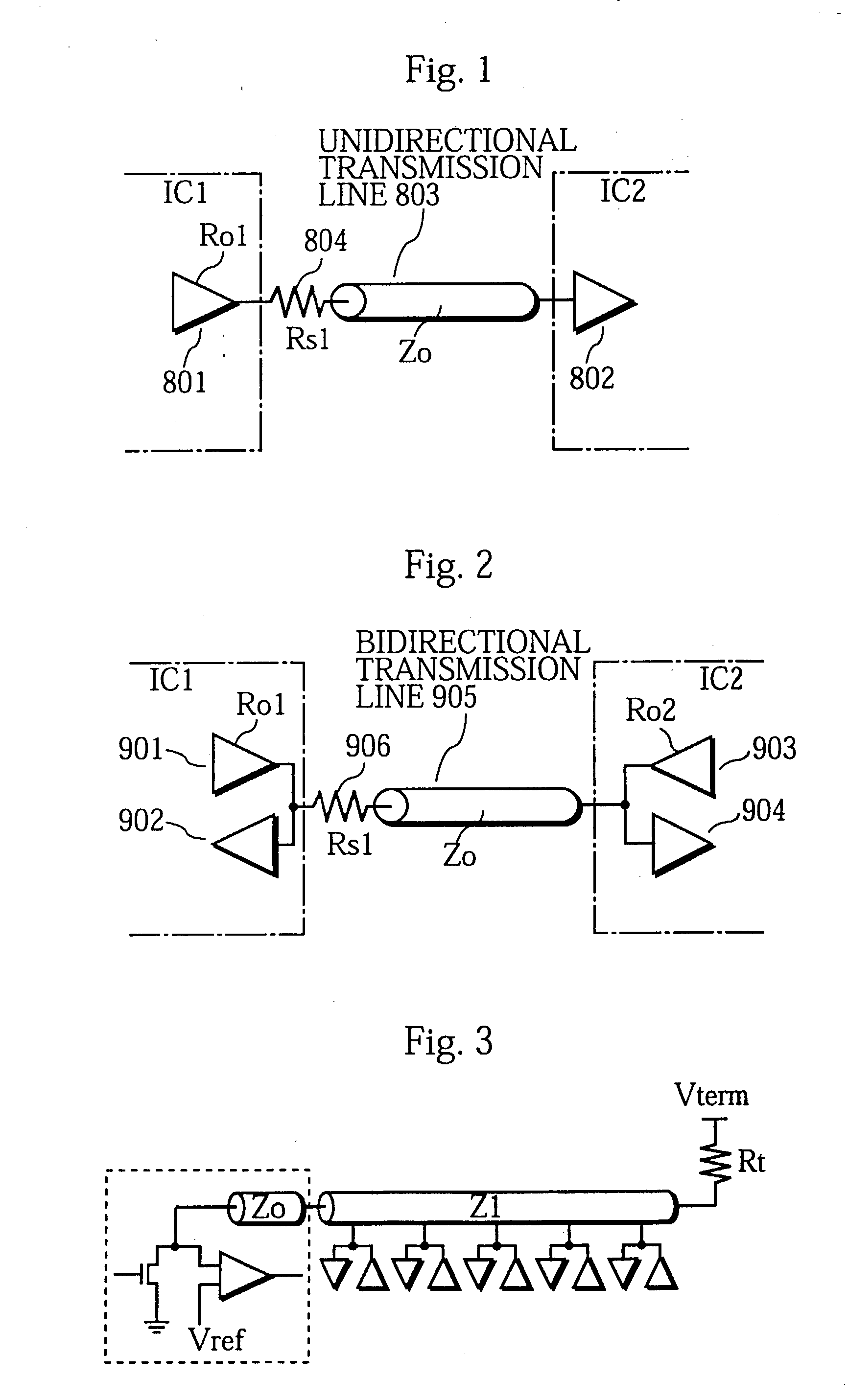
[0075] FIG. 7 shows the construction of a bidirectional signal transmission circuit according to the first embodiment of the invention. In the figure, a bidirectional transmission line 105 is a transmission line (whose characteristic impedance is Zo) for transmitting signals in two directions. This bidirectional transmission line 105 is one of bus lines constituting a bidirectional bus, such as a data bus, which connects semiconductor devices IC1 and IC2.

[0076] An I / O (Input / Output) circuit 120 is equipped within semiconductor device IC1 for inputting / outputting signals, and is mainly made up of an output buffer 101 (whose output resistance is Ro1) and an input buffer 102.

[0077] An I / O circuit 121 is equipped within semiconductor device IC2 for inputting / outputting signals, and is mainly made up of an output buffer 103 (whose output resistance is Ro2) and an input buffer 104.

[0078] A switching unit 106 assumes either of two states, namely series termination an...

second embodiment

[0090] Second Embodiment

[0091] FIG. 9 shows the construction of a bidirectional signal transmission circuit according to the second embodiment of the invention. This bidirectional signal transmission circuit differs with that shown in FIG. 7 in that switching units 301 and 303 have replaced the switching units 106 and 110. Construction elements which are the same as those in FIG. 7 have been given the same reference numerals and their explanation has been omitted, so that the following explanation will focus on the differences with the first embodiment.

[0092] The switching units 301 and 303 are different with the switching units 106 and 110 in that they are equipped respectively with buffer amplifiers 302 and 304 for amplifying signals instead of the resistors 108 and 112.

[0093] The buffer amplifier 302 is a buffer amplifier whose output resistance is approximately equal to the impedance Zo of the bidirectional transmission line 105. Accordingly, in the output of the I / O circuit 120...

third embodiment

[0097] Third Embodiment

[0098] FIG. 10 shows the construction of a bidirectional signal transmission circuit according to the third embodiment of the invention. This bidirectional signal transmission circuit differs with that shown in FIG. 7 in that switching units 401 and 403 have replaced the switching units 106 and 110. Construction elements which are the same as those in FIG. 7 have been given the same reference numerals and their explanation has been omitted, so that the following explanation will focus on the differences with the first embodiment.

[0099] In the switching units 401 and 403, series terminating resistors 108 and 112 have different resistances from those in the switching units, 106 and 110, and buffer amplifiers 402 and 404 for amplifying signals are newly equipped.

[0100] The buffer amplifiers 402 and 404 are arranged at stages immediately preceding the respective series terminating resistors 108 and 112 (i.e. on the sides of IC1 and IC2 with respect to the resistor...


PUM


Abstract

A bidirectional transmission circuit for inputting / outputting a signal from / onto a bidirectional transmission line includes: a transceiver for transmitting / receiving a signal; a first element having an impedance; a second element being a short line; and a switching unit for coupling the transceiver to the bidirectional transmission line via the first element when the transceiver transmits a signal, and coupling the transceiver to the bidirectional transmission line via the second element when the transceiver receives a signal.

Description

[0001] 1. Field of the Invention[0002] The present invention relates to a bidirectional signal transmission circuit and a bus system for facilitating impedance matching and fast signal transfer.[0003] 2. Description of the Prior Art[0004] As MPUs and memory devices become faster, the demand for speeding up data transfer on buses is growing in recent years. However, such speedups also incur difficulties in the proper transfer of data. This is because disturbances such as reflections of signals due to a mismatch with a characteristic impedance of a transmission line and crosstalk between adjacent lines become more serious with increase in data transfer rate.[0005] To avoid such unwanted signal reflections, impedance matching is commonly performed by means of series termination that inserts a resistor in series with a transmission line or parallel termination that inserts a resistor between a transmission line and a power or ground plane.[0006] The series termination couples a resistor...

Claims


Application Information

Patent Timeline
Patent Type & Authority Applications(United States)
IPC IPC(8): G06F13/40H04L5/16G06F13/38H04L25/02
CPCG06F13/4086H04L5/16H04L25/0292H04L25/028H04L25/0278G06F13/38
Inventor SHIBATA, OSAMUSAITO, YOSHIYUKIFUKUMOTO, YUKIHIRO
Owner PANASONIC CORP
Why Eureka
Try Eureka