

Method of cleaning processing chamber of semiconductor processing apparatus
a technology of processing chamber and processing apparatus, which is applied in the direction of cleaning hollow objects, cleaning using liquids, coatings, etc., can solve the problems of long cleaning time, complicated operation, and cracks in film and peeling o
Inactive Publication Date: 2003-11-06
TOKYO ELECTRON LTD
View PDF5 Cites 157 Cited by
- Summary
- Abstract
- Description
- Claims
- Application Information
AI Technical Summary
Problems solved by technology
When the thickness of the by-product film increases, the film cracks and peels off by, e.g., a temperature change in the processing chamber.
Consequently, the peeled by-product film turns into particles and is deposited on the wafer surface to cause device defects.
Unfortunately, these cleaning methods have the following drawbacks.
Method (a) requires a long cleaning time because wet cleaning is the main process.
Also, the method requires complicated operations, such as detachment, disassembly, attachment, and assembly of the constituent members.
This reduces the productivity because, e.g., the operating efficiency of the semiconductor processing apparatus lowers.
This hydrogen halide corrodes the metal of the casing of the processing chamber, and the produced metal halide scatters on the wafer to cause metal contamination.
Even if no water exists in the processing chamber, a halogen element remains in the processing chamber and corrodes the constituent members of the processing chamber in subsequent processes.
This results in an adverse effect, such as metal contamination of the wafer.
Unfortunately, these methods have the following drawbacks.
In method (c), etching is performed by the same type of gas as a process gas, but the process gas itself is not an optimal etchant.
That is, all metal elements cannot be removed, so the cleaning effect is limited.
In fact, according to Jpn. Pat. Appln. KOKAI Publication No. 5-144802, cleaning by the process gas is performed after the surface of an object is etched with a chemical, resulting in a complicated operation.
Also, this method cannot remove a thickly adhered by-product film, so the method cannot eliminate the cause of particle contamination.
That is, when this method is used, metal oxides build up in the processing chamber although cleaning is performed.
This limits the number of times of cleaning which can be performed by repeating this method alone.
Furthermore, this method cannot remove the by-product film itself either, so the method cannot eliminate the cause of particle contamination.
As described above, either of the conventional cleaning methods cannot well eliminate the cause of particle contamination and the cause of metal contamination.
Therefore, when either cleaning method is used, the reliability of semiconductor device fabrication worsens, and this consequently lowers the productivity and increases the production cost.
Method used
View moreImage
Smart ImageViewing Examples

Examples
Embodiment Construction
surface Upper 380 13 210 surface Comparative Lower 79 18 36 Example 2 surface Upper 52 10 20 surface Comparative Upper 42 7 10 Example 3 surface Comparative Upper 30 4 4.5 Example 4 surface
[0102] Additional advantages and modifications will readily occur to those skilled in the art. Therefore, the invention in its broader aspects is not limited to the specific details and representative embodiments shown and described herein. Accordingly, various modifications may be made without departing from the spirit or scope of the general inventive concept as defined by the appended claims and their equivalents.
Login to View More PUM
| Property | Measurement | Unit |
|---|---|---|
| temperature | aaaaa | aaaaa |
| temperature | aaaaa | aaaaa |
| temperature | aaaaa | aaaaa |
Abstract
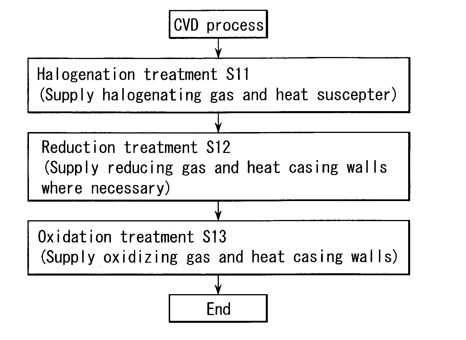
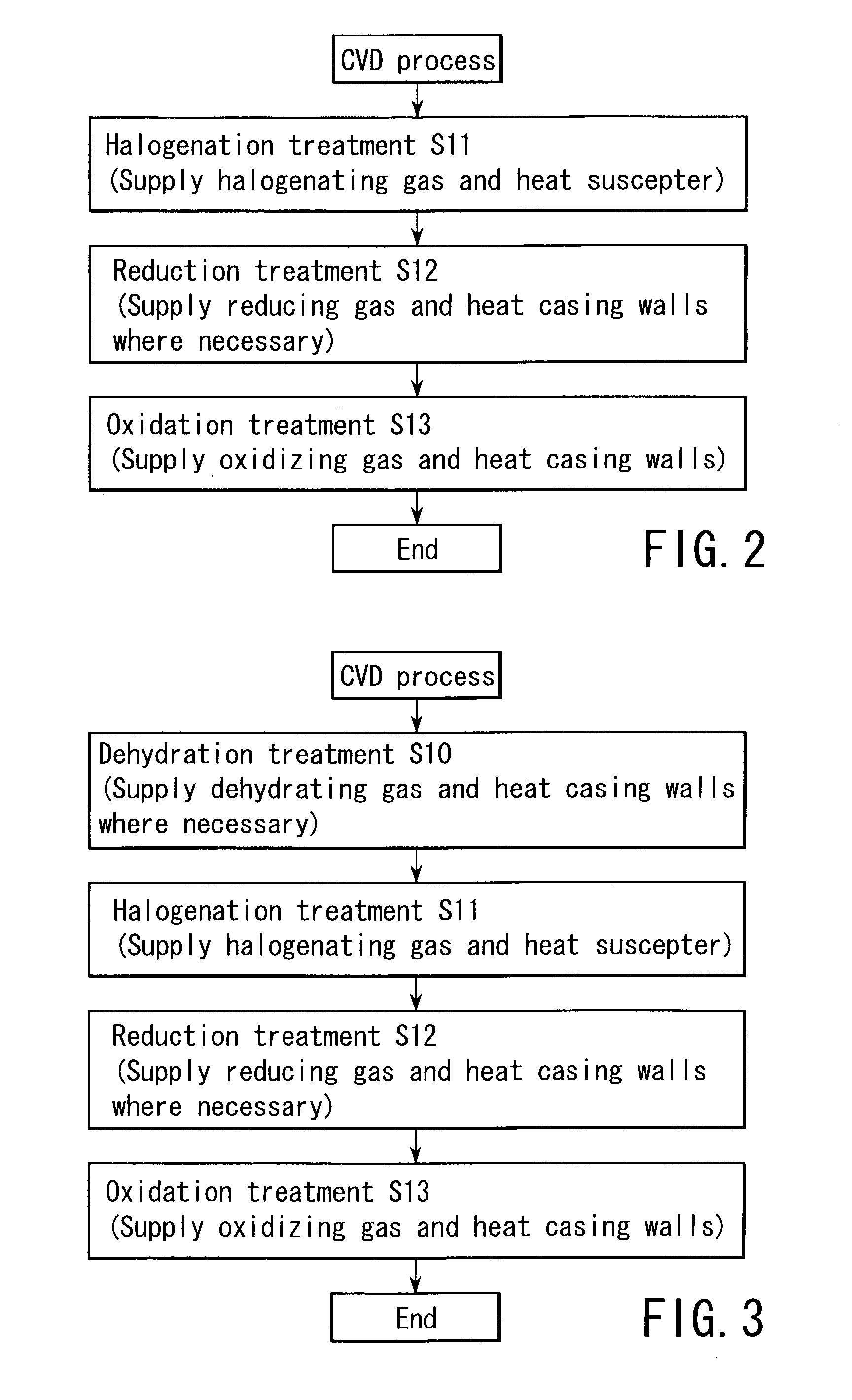
A method of cleaning the interior of a processing chamber first performs a halogenation treatment by supplying a treatment gas containing a halogenating gas into the processing chamber and heating a support member for a target substrate, thereby halogenating a metal element in a by-product film. A reduction treatment is then performed by supplying a treatment gas containing a reducing gas into the processing chamber, thereby reducing a halide of the metal element and liberating the metal element. An oxidation treatment is then performed by supplying a treatment gas containing an oxidizing gas into the processing chamber and heating the casing walls of the processing chamber, thereby passivating the liberated metal element by oxidation.
Description
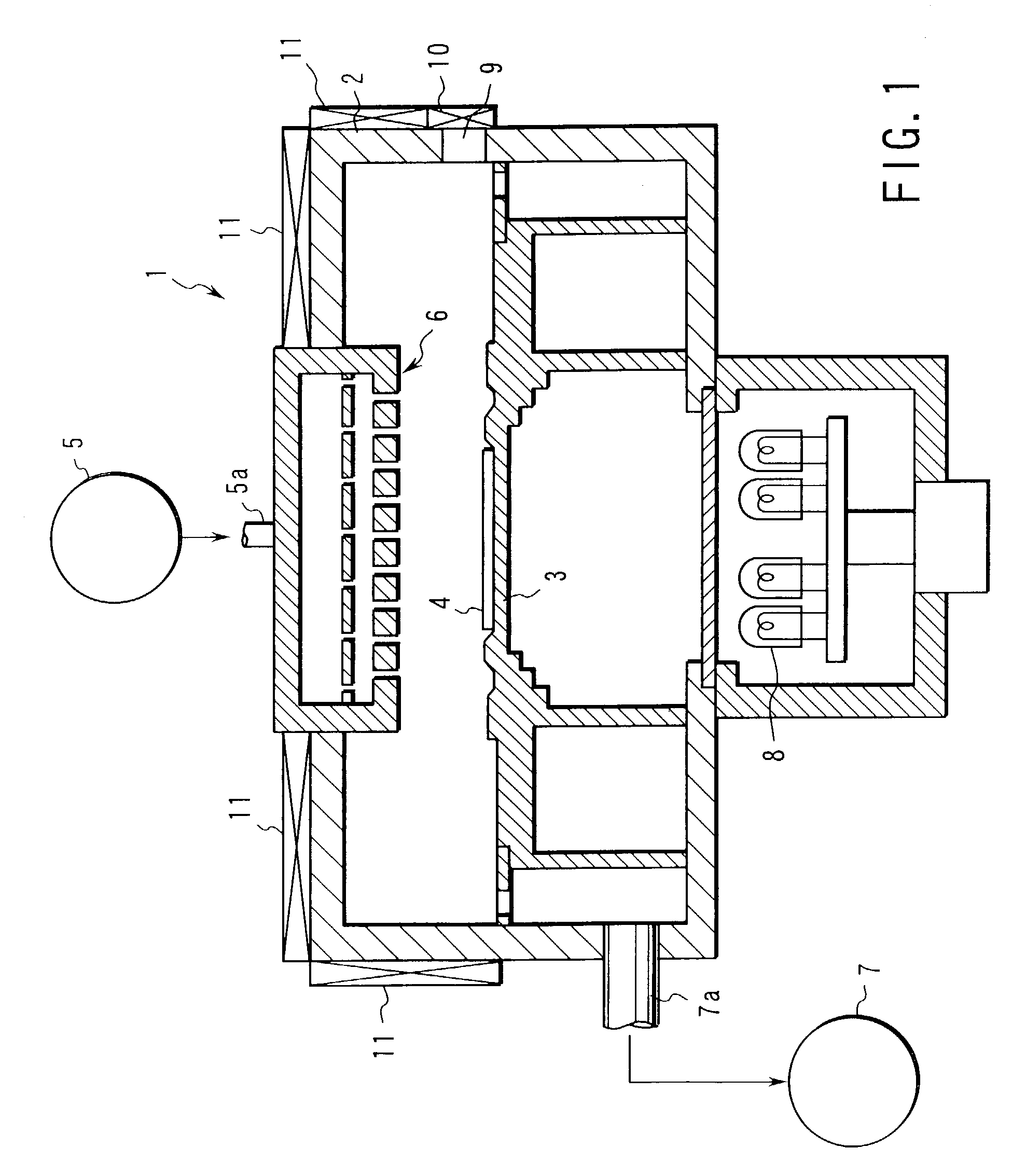
[0001] This is a Continuation-in-Part Application of PCT Application No. PCT / JP01 / 08515, filed Sep. 28, 2001, which was not published under PCT Article 21(2) in English.[0002] This application is based upon and claims the benefit of priority from the prior Japanese Patent Application No. 2000-353312, filed Nov. 20, 2000, the entire contents of which are incorporated herein by reference.[0003] 1. Field of the Invention[0004] The present invention relates to a method of cleaning a processing chamber of a semiconductor processing apparatus, e.g., a CVD (Chemical Vapor Deposition) apparatus. Note that "semiconductor processing" means various processes performed to form semiconductor layers, insulating layers, conductive layers, and the like into predetermined patterns on a target substrate, such as a semiconductor wafer or LCD substrate, thereby fabricating a structure including a semiconductor device and lines, electrodes, and the like connected to the semiconductor device on the subst...
Claims
Login to View More Application Information
Patent Timeline
 Patent Type & AuthorityApplications(United States)
IPC IPC(8): C23C16/44H01L21/205H01L21/302H01L21/3065H01L21/31
CPCC23C16/4405Y10S156/916
InventorSAKUMA, TAKESHI
OwnerTOKYO ELECTRON LTD