CMD and CMD-carrying CCD device

a ccd device and ccd technology, applied in the direction of radiation controlled devices, pulse techniques, counting chain synchronous pulse counters, etc., can solve the problem of difficult voltage control and fine control of signal amplification rate, and achieve the effect of uniform signal amplification ra

Inactive Publication Date: 2003-12-04
TEXAS INSTR INC
View PDF1 Cites 33 Cited by
  • Summary
  • Abstract
  • Description
  • Claims
  • Application Information

AI Technical Summary

Benefits of technology

[0012] In another aspect of this invention, by means of controlling change of the intermittent cycle of the first-phase driving voltage, one can adjust the period or round number of impact ionization for the signal charge transferred on the semiconductor substrate and beneath the electrode row, so that one can freely adjust the charge multiplication rate or signal amplification rate.
[0013] In a further aspect of this invention, if the number of cycles for applying said driving voltages in other phases during the period of passage of the signal charge of one pixel from one end to the other end of said plural electrodes is M, and the number of cycles of said driving voltages in other phases contained in 1 cycle of said first-phase driving voltage is N, N is a divisor of M. By meeting this condition, for the signal charges of all pixels passing through the CMD, the same number of rounds of intermittent impact ionization (charge multiplication) are carried out, and it is possible to obtain a uniform signal amplification rate free of dispersion.

Problems solved by technology

Consequently, fine control of the signal amplification rate by means of voltage control becomes very hard.

Method used


Image

  • CMD and CMD-carrying CCD device
  • CMD and CMD-carrying CCD device
  • CMD and CMD-carrying CCD device

Examples


Embodiment Construction

[0034] In the following, preferable embodiments of this invention will be explained with reference to FIGS. 1-9.

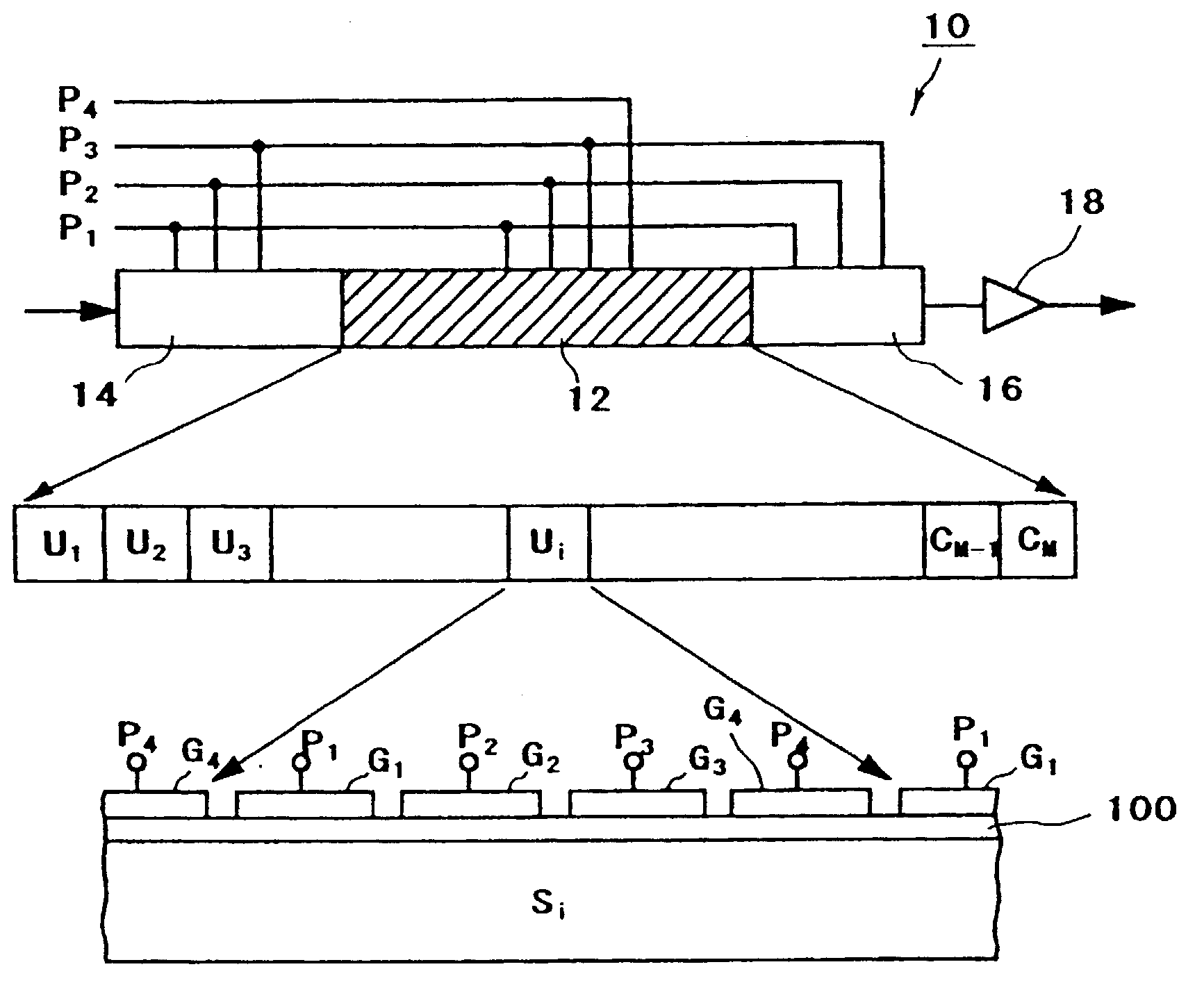
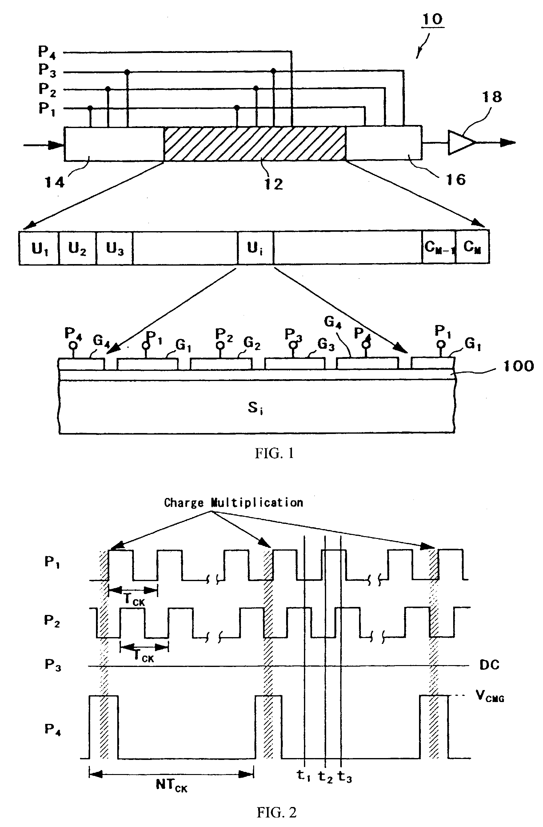
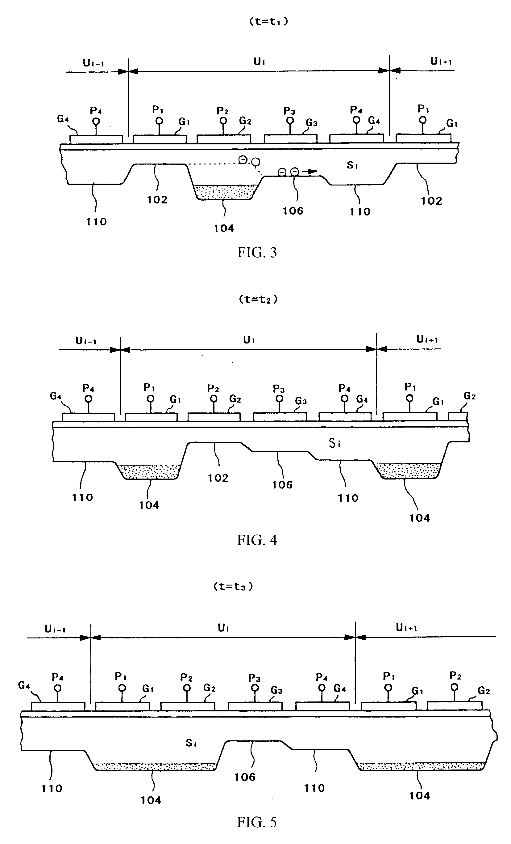
[0035] FIG. 1 is a diagram illustrating the basic constitution of the CMD-carrying CCD device in an embodiment of this invention. As shown in the figure, this CMD-carrying CCD device 10 has a CCD 14, 16 connected in series to the former portion (input side) and / or latter portion (output side) of CMD 12. In this case, CMD 12 and CCD 14, 16 may be formed in the same process on a single or common semiconductor substrate. On the surface of the substrate, the signal charge is transferred directly from beneath the electrode on the output end of former-portion CCD 14 to beneath the electrode on the input end of CMD 12, and the signal charge is directly transferred from beneath the electrode of the output end of CMD 12 to beneath the electrode on the input end of latter-portion CCD 16. On the output end of latter-portion CCD 16, an output portion is set for converting the signal c...


PUM


Abstract

This invention controls the signal amplification rate in a simple way with high precision in a CMD or CMD-carrying CCD device. CMD 12 has plural sections, such as M sections (U1-UM), each of which is a CMD unit U that can perform a charge multiplication operation, set in series. Each section of CMD unit Ui has plural (such as 4) electrodes G1, G2, G3, G4 set in a row via an insulating film, such as silicon oxide film 100, on a silicon insulating film. Among driving voltages P1, P2, P3, P4 applied on the electrodes G1, G2, G3 and G4, P1 and P2 are applied in the same cycle as the transfer clock, P4 for impact ionization is applied in intermittent cycles with respect to P1 and P2, and P3 is applied as a DC voltage at a prescribed level.

Description

[0001] This invention pertains to a CCD (Charge Coupled Device). More specifically, this invention pertains to a CMD (Charge Multiplying Device).[0002] It is well known that a CCD is a semiconductor device that can store signal charges near the surface of a semiconductor substrate and transfer said signal charges in succession. On the other hand, a CMD is described in the invention of U.S. Pat. No. 5,337,340 published on Aug. 9, 1994, and it is a semiconductor device that uses a CCD and can realize a charge multiplication or signal amplification function inside the CCD cell.[0003] FIG. 10 is a diagram illustrating the constitution of a CMD. As shown in the figure, as the basic unit of the CMD or CMD unit U.sub.CMD, a plurality (say, 4) electrodes G1, G2, G3, G4 are set in a row via an insulating film, such as silicon oxide film 100, on a silicon substrate. Driving voltages P1, P2, P3, P4 with phase and cycle relationships shown in FIG. 11 are applied on said electrodes G1, G2, G3, G...

Claims


Application Information

Patent Timeline
Patent Type & Authority Applications(United States)
IPC IPC(8): G11C11/35G11C19/28H01L29/762H01L21/339H01L27/148H04N5/335H04N5/369H04N5/372
CPCG11C19/282
Inventor KASHIMA, SHUNJIYAHATA, KYOICHIKOBAYASHI, IZUMI
Owner TEXAS INSTR INC
Why Eureka
Try Eureka