Method and apparatus for inspecting defects

Active Publication Date: 2003-12-11
SUMITOMO MITSUBISHI SILICON CORP
View PDF2 Cites 29 Cited by
  • Summary
  • Abstract
  • Description
  • Claims
  • Application Information

AI Technical Summary

Problems solved by technology

Thus it takes a lot of time for an operator to perform the inspection.
However, the inspection techniques disclosed by the above two publications have still difficult situations as below.
Hence, this inspection technique has still suffered from the problem that it takes a lot of time to scan the whole area of a surface to be inspected of an object such as a silicon wafer.
This makes it difficult to distinguish the blots or others from the defects.
As a result, during a final inspection step carried out at higher magnifications, there often occurs the necessity of re-imaging the whole area of the surface of the object, which will reduce the efficiency of inspection.
Howev

Method used


Image

  • Method and apparatus for inspecting defects
  • Method and apparatus for inspecting defects
  • Method and apparatus for inspecting defects

Examples


Example

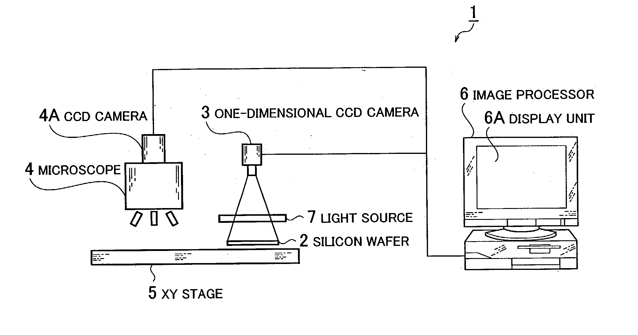
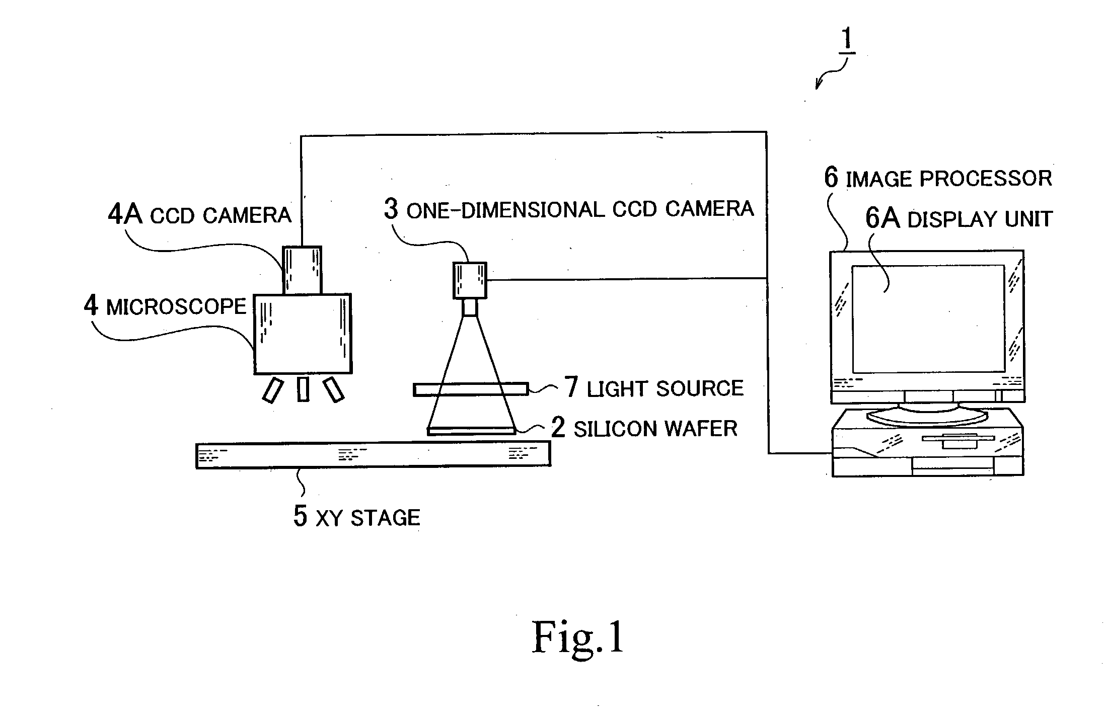
[0074] An example will now be described with reference to practical numerical values concerning the defect inspection apparatus 1.

[0075] Imaging conditions for the one-dimensional CCD camera 3 includes the number of pixels of 4096 and a scan rate of 1 kHz. As shown in FIG. 4, the width of a field of view of the one-dimensional CCD camera 3 is 210 mm which is in accord with a silicon wafer of 8 inches. The silicon wafer 2 is conveyed by the XY stage 5 at a speed of 50 mm / sec. A linear light source 7 is used as illumination means.

[0076] Accordingly, the one-dimensional CCD camera 3 is able to image an object at a resolution of 0.051 (mm / pixel) (=210 (mm) / 4096 (pixels)) in its width direction of the field of view.

[0077] In the conveyance direction of the silicon wafer 2, a range of 0.05 (mm) (=50 (mm / sec) / 1000 (Hz)) can be imaged per one time of scanning carried out by the one-dimensional CCD camera 3. Image signals resultant from each time of scanning are stored in an image memory in ...


PUM


Abstract

Provided are a method and apparatus for inspecting a defect on a plane, such as a surface or a section, of an object to be inspected. The object is, for instance, a silicon wafer. A whole area of a plane of the object is first imaged by an optical system to gain image signals. Then, a particular region on the plane is positionally detected from the image signals. The particular region includes a blot and a defect and has a higher luminance than a remaining region on the plane. A blot is distinguishably detected from the particular region. A specified region on the plane is then subjected to a detailed inspection under a microscope. The region is set to avoid the blot even if the blot is on the region. The detailed inspection under the microscope is performed toward only the region with no blot.

Description

[0001] 1. Technical Field of the Invention[0002] The present invention relates to a method and an apparatus for inspecting defects on a surface or section of an object to be inspected, such as a silicon wafer.[0003] 2. Related Art[0004] A microscopic inspection for possible detects on a surface or section of an object to be inspected, such as a silicon wafer, has already been carried out. Because the field of view of a normally used microscope is approximately a several-millimeters square, inspecting a whole area of a surface to be inspected, for example, of a silicon wafer requires that the field of view of the microscope be moved several tens of times or several hundreds of times repeatedly. Thus it takes a lot of time for an operator to perform the inspection.[0005] The technique for overcoming such a situation has been proposed by Japanese patent laid-open (unexamined) publications 11(1999)-354599 and 2001-183301.[0006] In the former publication, a differential interference micr...

Claims


Application Information

Patent Timeline
IPC IPC(8): G01N21/956G01N21/64G01N21/95H01L21/66
CPCG01N21/9501G01N21/6489G01N2021/8867
Inventor YOKOYAMA, HIROKAZUMURAKAMI, HIROKI
Owner SUMITOMO MITSUBISHI SILICON CORP
Why Eureka
Try Eureka