Electron beam exposure or system inspection or measurement apparatus and its method and height detection apparatus

a technology of electromagnetic radiation and exposure, applied in the field of electromagnetic radiation exposure, can solve the problems of affecting affecting the accuracy so as to improve the quality of the electron beam image, reduce the resolution, and reduce the effect of electron optical system deflection and aberration

Inactive Publication Date: 2005-07-19
HITACHI LTD
View PDF12 Cites 25 Cited by
  • Summary
  • Abstract
  • Description
  • Claims
  • Application Information

AI Technical Summary

Benefits of technology

[0008]It is therefore an object of the present invention is to provide an electron beam exposure or system inspection or measurement apparatus and a method thereof in which the image distortion caused by the deflection and the aberration of the electron optical system can be reduced, the decrease of the resolution due to the de-focusing can be reduced so that the quality of the electron beam image (SEM image) can be improved and in which the inspection and the measurement of length based on the electron beam image (SEM image) can be executed with high accuracy and with high reliability.
[0009]It is another object of the present invention is to provide an electron beam exposure or system inspection or measurement apparatus and a method thereof in which the height of the surface of the inspected object can be detected real time and the electron optical system can be controlled real time so that an electron beam image (SEM image) of high resolution without image distortion can be obtained by the continuous movement of the stage, an inspection efficiency and its stability can be improved and in which an inspection time can be reduced.
[0010]It is a further object of the present invention to provide an electron beam exposure apparatus and a converging ion beam manufacturing apparatus in which very small patterns can be exposed and manufactured without image distortion and with a high resolution.

Problems solved by technology

This process requires a lot of time, and also, a sample surface is scanned by electron beams many times. Accordingly, there is the possibility that a sample will be damaged.
It takes a lot of time to measure an optimum control current before inspection.
Moreover, there is the risk that a sample will be damaged due to the irradiation of electron beams for a long time.
Further, there is the problem that a height of a sample surface will be changed depending upon a method of holding a wafer during the inspection.
According to the above-mentioned prior art, in the electron beam apparatus, the point in which a clear SEM image without image distortion is detected and a defect of a very small pattern formed on the inspected object like a semiconductor wafer such as ULSI or VLSI is inspected and a dimension of a very small pattern is measured with high accuracy and with high reliability has not been considered sufficiently.

Method used


Image

  • Electron beam exposure or system inspection or measurement apparatus and its method and height detection apparatus
  • Electron beam exposure or system inspection or measurement apparatus and its method and height detection apparatus
  • Electron beam exposure or system inspection or measurement apparatus and its method and height detection apparatus

Examples


second embodiment

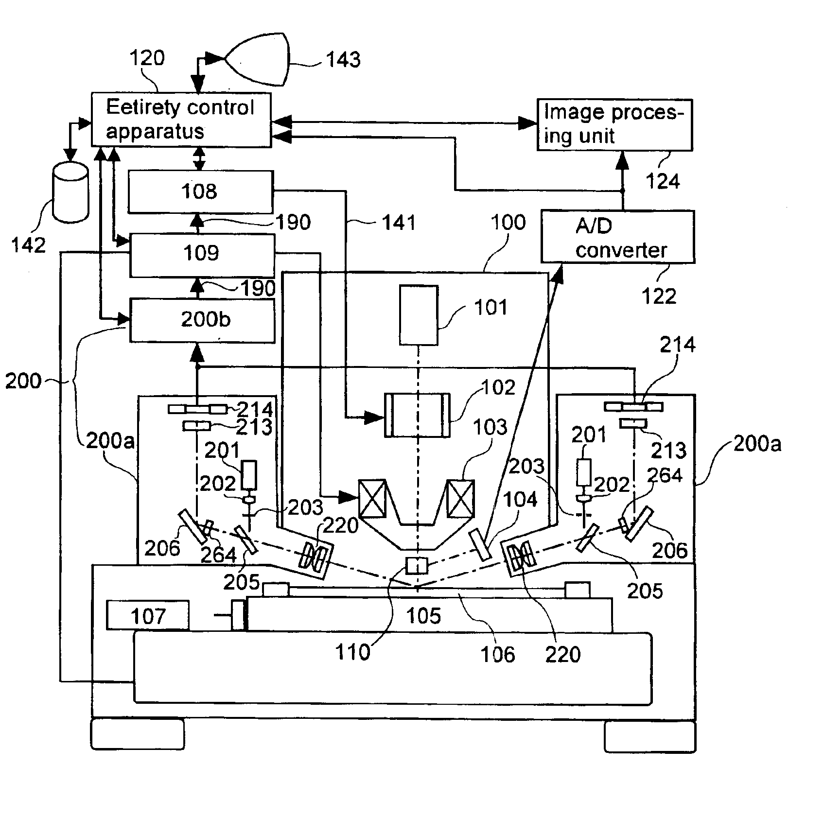
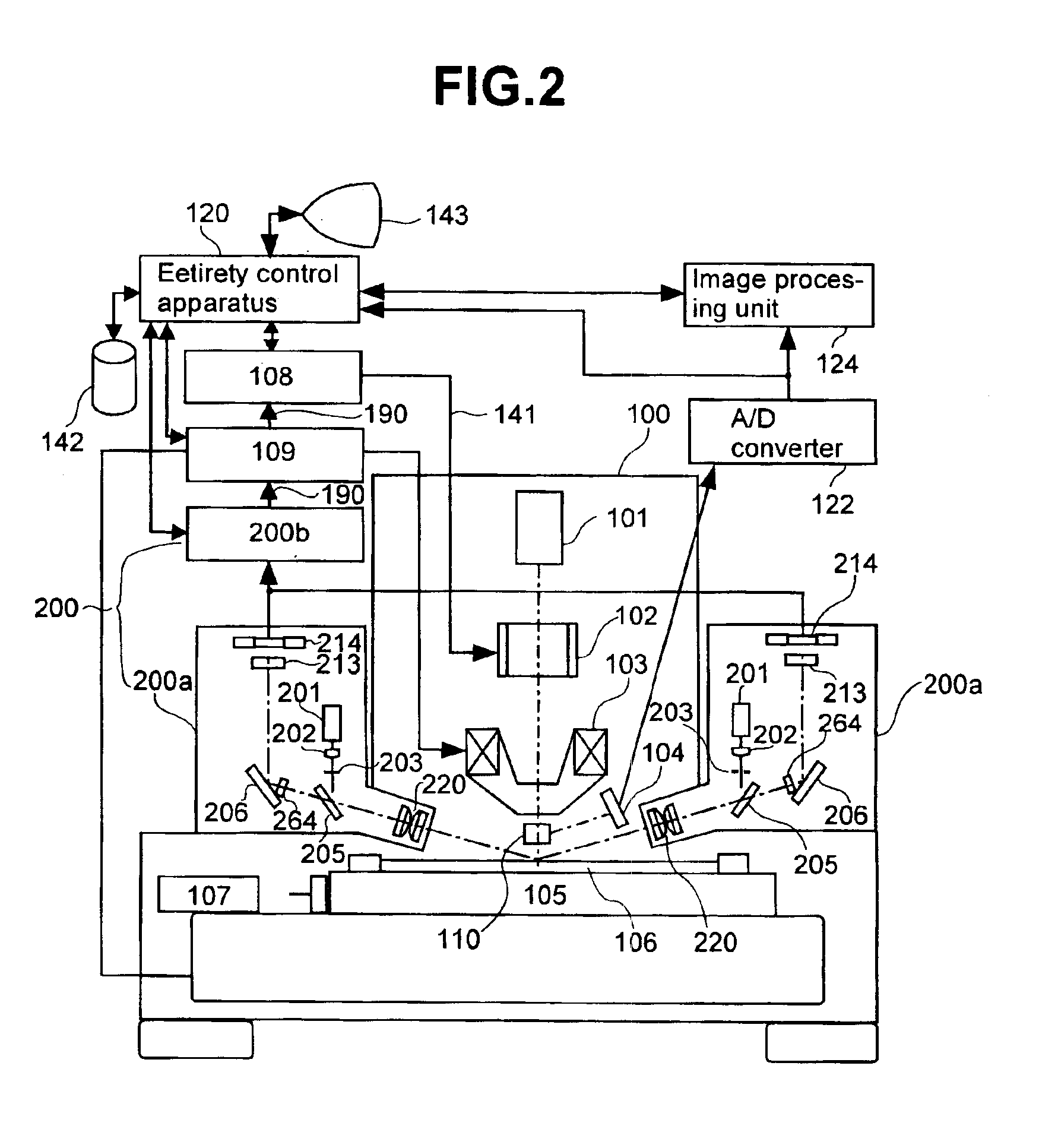
[0087]The height detection apparatus 200 composed of the height detection optical apparatus 200a and the height calculating unit 200b is arranged substantially similarly to a second embodiment which will be described later, and is installed about an optical axis 110 of an electron beam symmetrically with respect to the sample 106. An illumination optical system of each height detection optical apparatus 200a comprises a light source 201, a condenser lens 202, a mask 203 with a multi-slit pattern, a half mirror 205, and a projection / detection lens 220. A detection optical system of each height detection optical apparatus 200a comprises a projection / detection lens 220, a magnifying lens 264 for focusing an intermediate multi-slit image focused by the projection / detection lens 220 on a line image sensor 214 in an enlarged scale, a mirror 206, a cylindrical lens (cylindrical lens) 213, and a line image sensor 214.

[0088]By the illumination optical system of the respective height detectio...

first embodiment

[0152]FIGS. 10 and 11(a)-11(b) show the height detection optical apparatus 200a according to the present invention. Specifically, the height detection optical apparatus 200a according to the present invention comprises an illumination optical system formed of a light source 201, a mask 203 in which the same pattern irradiated with light from the light source 201, e.g. the pattern composed of repetitive (repeated) rectangular patterns, a projection stop 211, a polarizing filter 240 for emitting S-polarized light and a projection lens 210 and which illuminates the multi-slit shaped pattern with the S-polarized light at an angle (θ=greater than 60 degrees) vertically inclined from the sample surface 106 by an angle θ and a detection optical system composed of a detection lens 215 for focusing regularly-reflected light from the sample surface 106 on the light-receiving surface of a line image sensor 214, a cylindrical lens 213 and a detection lens 216 for converging the longitudinal dir...


PUM

PropertyMeasurementUnit
angleaaaaaaaaaa
incident angleaaaaaaaaaa

Abstract

An electron beam apparatus including a table which mounts a specimen and is movable in three dimensional directions, an electron beam optical system irradiating an electron beam onto a specimen and for detecting a secondary electron emanated from the specimen by the irradiation of the electron beam, and a surface height detection system for detecting height of the surface of the specimen mounted on the table. A focus control system controls a relative position between a focus position of the electron optical system and the table in accordance with information of the height, and an image processing system obtains an image from the detected secondary electron and processes the obtained image to detect a defect on the surface of the specimen.

Description

CROSS REFERENCE TO RELATED APPLICATION[0001]This is a continuation of U.S. application Ser. No. 10 / 012,454, filed Dec. 12, 2001, now U.S. Pat. No. 6,753,518, which is a continuation of U.S. application Ser. No. 09 / 642,014, filed Aug. 21, 2000, now U.S. Pat. No. 6,333,510, which is a continuation of U.S. application Ser. No. 09 / 132,220, filed Aug. 11, 1998, now U.S. Pat. No. 6,107,637, the subject matter of which is incorporated by reference herein.BACKGROUND OF THE INVENTION[0002]The present invention relates to an electron beam exposure or system inspection or measurement or processing apparatus having an observation function using charged particle beams such as electron beams or ion beams and its method and an optical height detection apparatus.[0003]Heretofore, a focus of an electron microscope has been adjusted by adjusting a control current of an objective lens while an electron beam image is observed. This process requires a lot of time, and also, a sample surface is scanned b...

Claims


Application Information

Patent Timeline
Patent Type & Authority Patents(United States)
IPC IPC(8): H01J37/30H01J37/02H01J37/21H01J37/304G01Q30/04G01Q30/20G21K7/00
CPCB82Y10/00B82Y40/00H01J37/20H01J37/21H01J37/222H01J37/226H01J37/265H01J37/28H01J37/304H01J37/3174H01J2237/20235H01J2237/20292H01J2237/216H01J2237/2445H01J2237/24578H01J2237/2482H01J2237/2487H01J2237/2814H01J2237/2817H01J2237/2826H01J2237/304H01J2237/3175
Inventor WATANABE, MASAHIROHIROI, TAKASHITANAKA, MAKISHINADA, HIROYUKIUSAMI, YASUTSUGU
Owner HITACHI LTD
Why Eureka
Try Eureka