Methods for fabricating three-dimensional all organic interconnect structures

a three-dimensional all organic, interconnected technology, applied in the direction of thermal polymer dielectrics, inductances, printed circuit assembling, etc., can solve the problems of high density requirements for multi-layer circuits, high frequency applications becoming ever more demanding, and the unresolved need for a low cost multi-layer process

Inactive Publication Date: 2004-01-01
GEORGIA TECH RES CORP
View PDF94 Cites 94 Cited by
  • Summary
  • Abstract
  • Description
  • Claims
  • Application Information

AI Technical Summary

Problems solved by technology

The requirements for multilayer circuits in high density, high performance applications are becoming ever more demanding for high frequency applications.
As a result there exists an unresolved need for a low cost multilayer process that can support both high frequency and high density (e.g., fine line and spaces, small via sizes) multilayer circuit constructions.

Method used


Image

  • Methods for fabricating three-dimensional all organic interconnect structures
  • Methods for fabricating three-dimensional all organic interconnect structures
  • Methods for fabricating three-dimensional all organic interconnect structures

Examples


Embodiment Construction

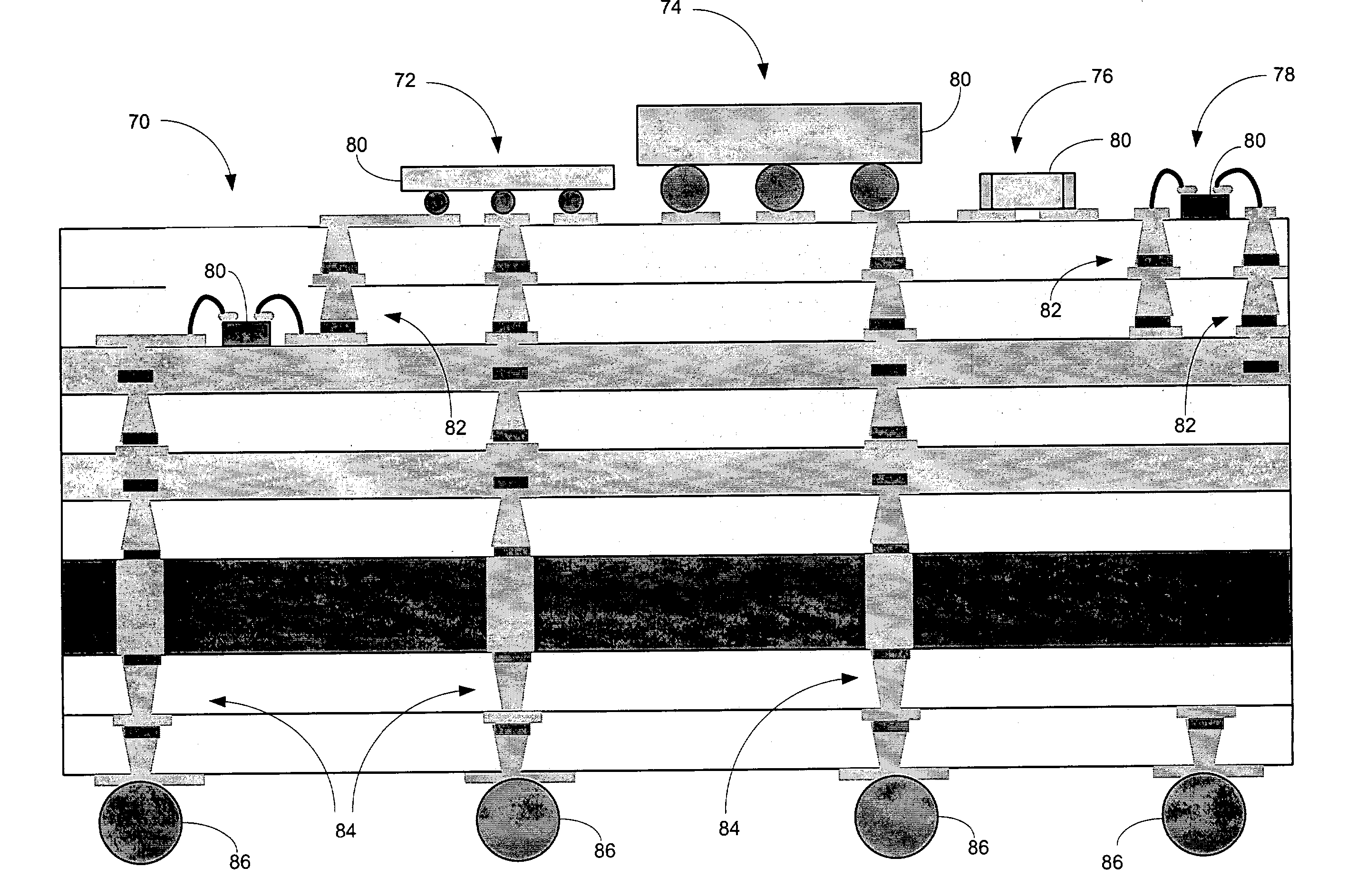
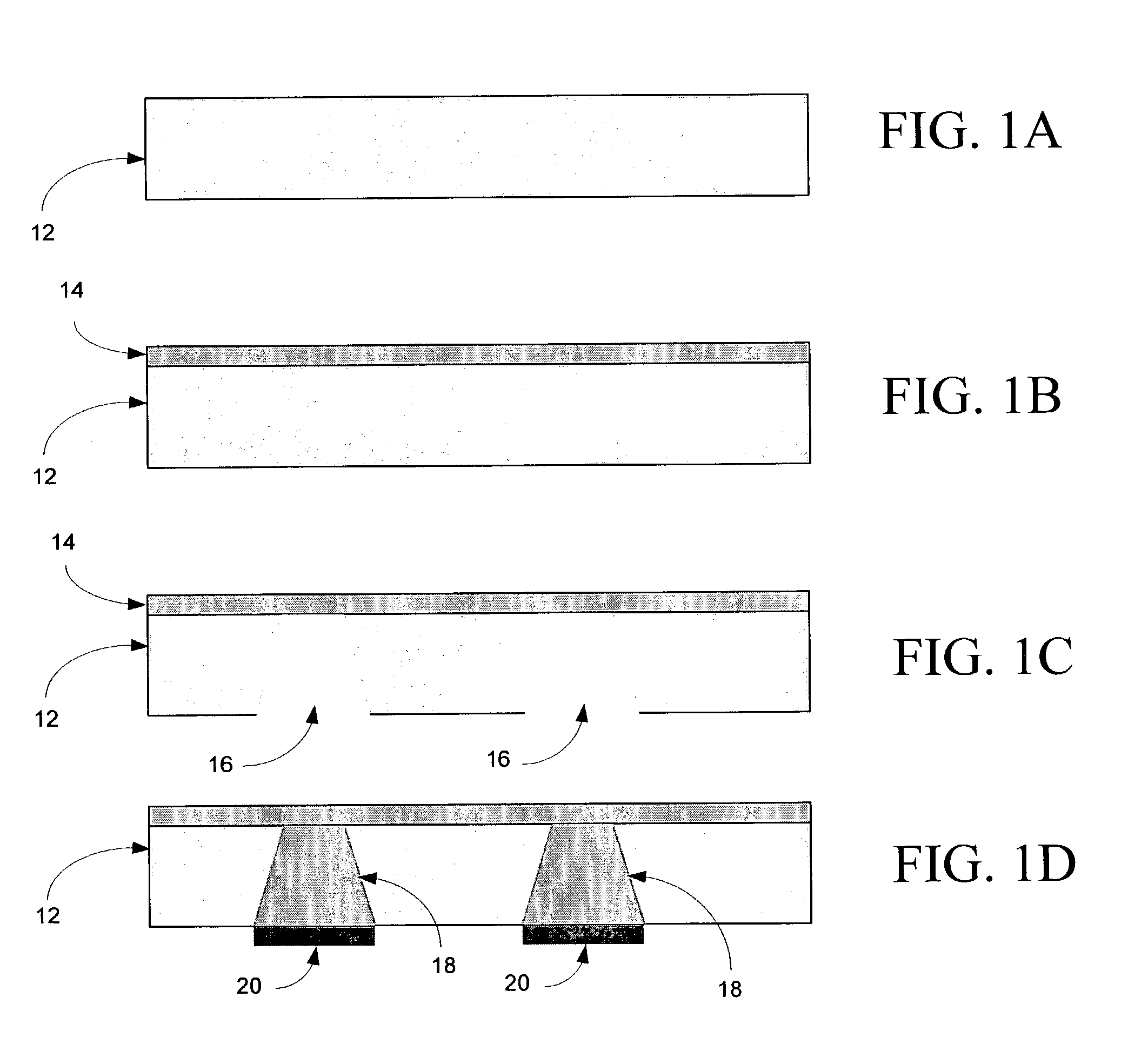
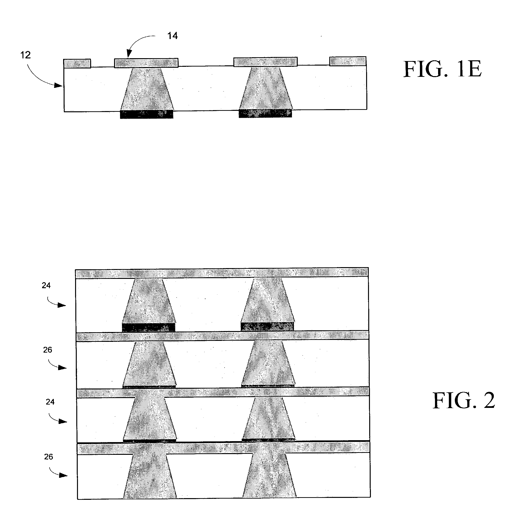
[0030] The following is an illustrative embodiment of a method of fabricating a multilayer organic structure according to the present invention utilizing LCP as the organic material, followed by several alternative embodiments.

[0031] FIG. 1A is a schematic representation of an uncladded high temperature or low temperature LCP dielectric film 12, in accordance with an embodiment of the present invention. In a preferred embodiment, the high and low temperature LCP film has a CTE between 2 and 20 ppm / .degree. C.

[0032] Next, as illustrated in FIG. 1B, a metalized layer 14 has been fabricated on the high temperature or low temperature LCP dielectric film 12, in accordance with an embodiment of the present invention. Metallization of the LCP film 12 can be accomplished by electroless and electroplating, sputtering, evaporation, or chemical vapor deposition. Metallization can be an adhesive metal such as copper, chromium, titanium, or platinum, followed by deposition of either copper, nick...


PUM

PropertyMeasurementUnit
thicknessaaaaaaaaaa
dielectric constantsaaaaaaaaaa
volume fractionaaaaaaaaaa

Abstract

The present invention comprises methods for making three-dimensional (3-D) liquid crystalline polymer (LCP) interconnect structures using a high temperature singe sided liquid crystalline polymer, and low temperature single sided liquid crystalline polymer, whereas both the high temperature LCP and the low temperature LCP are drilled using a laser or mechanical drill or mechanically punch to form a z-axis connection. The single sided Conductive layer is used as a bus layer to form z axis conductive stud conductive stud within the high temperature and low temperature LCP, followed by deposition of a metallic capping layer of the stud that serves as the bonding metal between the conductive interconnects to form the z-axis electrical connection. High temperature and low temperature LCP circuit layers are etched or built up to form circuit patterns and subsequently bonded together to form final 3-D multilayer circuit pattern whereas the low temperature LCP melts to form both dielectric to dielectric bond to high temperature LCP circuit layer, and dielectric to conductive bond, whereas, metal to metal bonding occurs with high temperature metal capping layer bonding to conductive metal layer. The resultant structure is then packaged using two metallized organic cores that are laminated onto either side of the device using a low temperature adhesive with similar electrical properties and subsequently metallized to form the input output terminals and EM shielding.

Description

[0001] This application claims benefit of co-pending U.S. Provisional Application No. 60 / 391,742, filed Jun. 26, 2002, which is entirely incorporated herein by reference. In addition, this application is related to the following co-pending, commonly assigned U.S. applications, each of which is entirely incorporated herein by reference: "Integrated Passive Devices Fabricated Utilizing Multilayer, Organic Laminates" filed Mar. 28, 2003, and accorded Application No. ______; and "Stand-Alone Organic-Based Passive Devices" filed Mar. 28, 2003, and accorded Application No. ______.[0002] I. Field of the Invention[0003] The present invention generally relates to three-dimensional all organic structures, and more particularly to three-dimensional organic interconnect structures for use in radio frequency and mixed signal module substrates and multilayer high-speed printed circuit boards.[0004] II. Description of Related Art[0005] Multilayer circuits typically comprise at least one conductive...

Claims


Application Information

Patent Timeline
Patent Type & Authority Applications(United States)
IPC IPC(8): H01F17/00H01F41/04H01L21/48H01L25/065H01L27/08H05K1/16H05K3/46
CPCH01F17/0033Y10T29/49149H01L21/4857H01L25/0652H01L27/08H01L2224/16H01L2224/48235H01L2924/01012H01L2924/01046H01L2924/01078H01L2924/01079H01L2924/15311H01L2924/19041H01L2924/19105H01L2924/3011H01L2924/3025H05K1/162H05K1/167H05K3/4617H05K3/4632H05K3/4688H05K2201/0129H05K2201/0141H05K2201/0209H01L2924/01019H01L2224/16235Y10T29/49158Y10T29/49126H01F41/041H01L2924/00014H01L2224/0401H01L21/48H01L23/498H05K1/02H05K3/46B32B37/00H05K1/00
Inventor WHITE, GEORGE E.SWAMINATHAN, MADHAVANSUNDARAM, VENKATESHDALMIA, SIDHARTH
Owner GEORGIA TECH RES CORP
Why Eureka
Try Eureka