Time recording device and a time recording method employing a semiconductor element

a time recording device and semiconductor element technology, applied in the field of time recording devices and methods, can solve the problems of shifting in the centre of charge concentration, electronic circuit or chipcard ic vulnerable to unauthorized access,

Inactive Publication Date: 2004-02-19
INFINEON TECH AG
View PDF6 Cites 22 Cited by
  • Summary
  • Abstract
  • Description
  • Claims
  • Application Information

AI Technical Summary

Benefits of technology

[0010] a semiconductor element with a transistor structure, which includes source / drain regions and a channel region between the same, a gate dielectric arranged above the channel region, a floating gate electrode arranged above the gate dielectric, a layer sequence comprising an oxide layer arranged on the floating gate electrode and a nitride layer arranged on the oxide layer, the layer sequence being arranged above the floating gate electrode, and a control gate electrode arranged above the layer sequence;
[0012] a unit for recording a time which has elapsed since charge injection on the basis of changes in the transmission behaviour of the channel region caused by a shift in the centre of concentration of the charges in the nitride layer away from the interface.
[0014] applying a voltage or voltage pulses to the control gate electrode of a semiconductor element having a transistor structure, which includes source / drain regions; a channel region between the same; a gate dielectric arranged above the channel region; a floating gate electrode arranged above the gate dielectric; a layer sequence comprising an oxide layer arranged on the floating gate electrode and a nitride layer arranged on the oxide layer, the layer sequence being arranged above the floating gate electrode; and the control gate electrode arranged above the layer sequence, so as to inject charges into the floating gate electrode and into the nitride layer, a centre of concentration of the charges injected into the nitride layer being located at the interface between the oxide layer and the nitride layer of the layer sequence; and
[0007] From U.S. Pat. No. 5,760,644 an integrated semiconductor circuit is known by means of which a time lapse can be recorded. According to U.S. Pat. No. 5,760,644 charge carriers are introduced for this purpose into a storage dielectric and changes in the electric field arising from the charge introduced into the dielectric are used for time recording. This electric field changes with increasing natural charge diminution in the dielectric material, so that measurement of the electric field with time provides information on the time which has elapsed. The storage dielectric used in U.S. Pat. No. 5,760,644 is the ONO structure (oxide-nitride-oxide structure) of an SONOS transistor (silicon-ONO-silicon transistor) or the NO structure (nitride-oxide structure) of an SNOS transistor (silicon-NO-silicon transistor). Using the ONO dielectric or the NO dielectric of the above storage transistors, the time-dependent charge loss of the electrons stored in the nitride is established through the altered effective voltage of the cell.

Problems solved by technology

A successful attack, which would make the electronic circuit or the chipcard IC vulnerable to an unauthorized access, requires a certain number of switchon events.
Later these charge carriers begin to wander through the nitride due to a trap-supported conduction mechanism, known as hopping conduction, which results in a shift in the centre of charge concentration.
Charge injection into the ON isolation layer sequence or the ONO isolation layer sequence is here simply an undesirable side effect.

Method used


Image

  • Time recording device and a time recording method employing a semiconductor element
  • Time recording device and a time recording method employing a semiconductor element
  • Time recording device and a time recording method employing a semiconductor element

Examples


Embodiment Construction

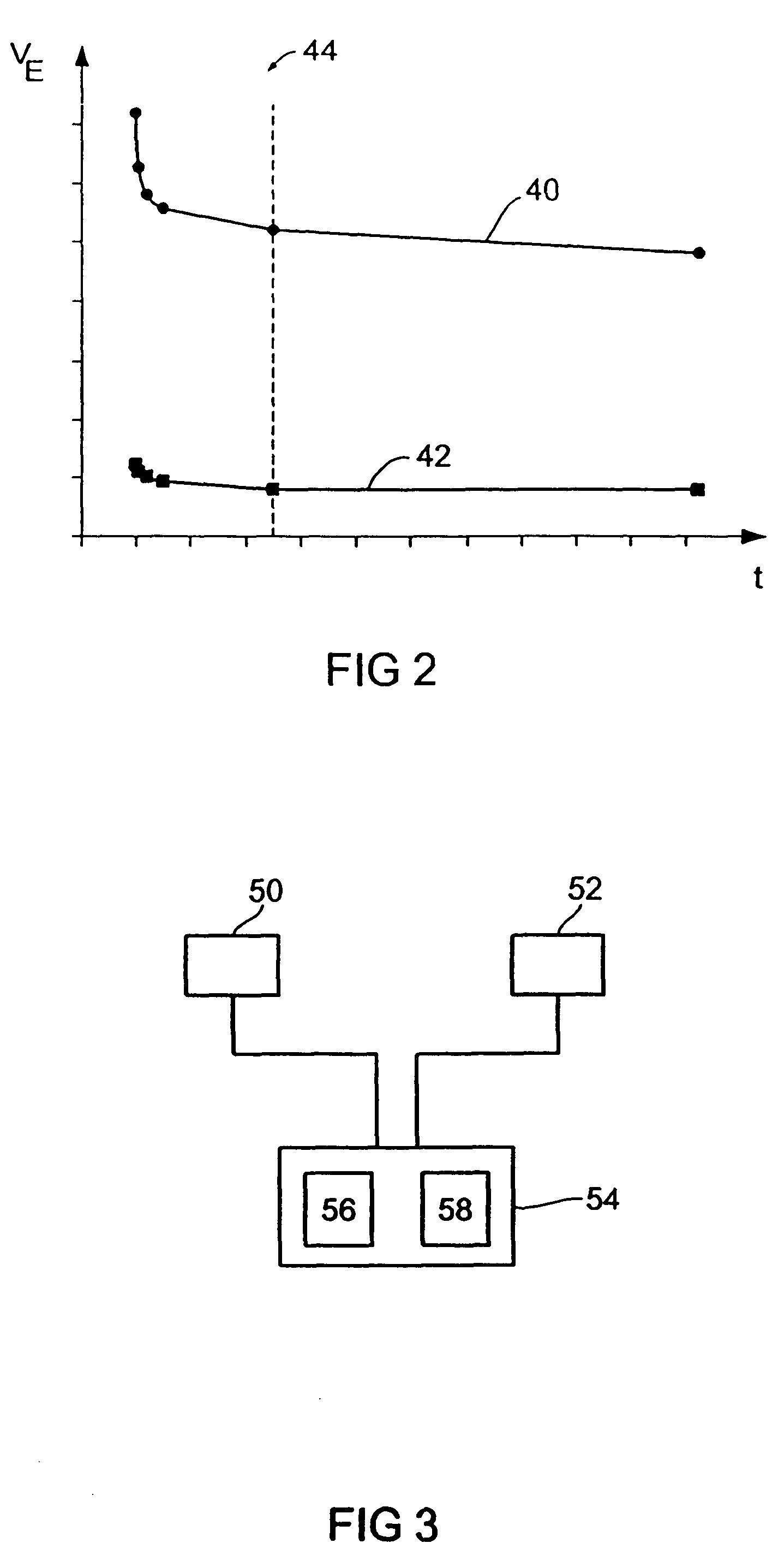
[0025] Before giving a more detailed description of the effect on which time recording according to the present invention is based, i.e. a shift in the centre of charge concentration in the nitride layer of a semiconductor element with a transistor structure, which is an EEPROM storage cell in preferred embodiments of the present invention, making reference to FIGS. 2 and 3, the structure of such an EEPROM storage cell will first be outlined briefly.

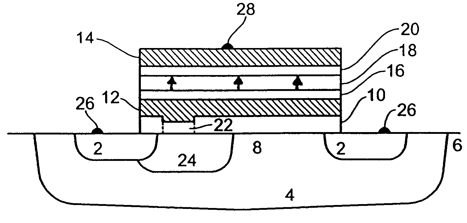
[0026] FIG. 1 shows a schematic cross-sectional view of such an EEPROM storage cell, wherein source / drain regions 2 are provided by suitable implantation in the doped well 4 of a semiconductor substrate 6. Above the channel region 8 of the storage cell located between the source / drain regions a gate oxide 10 is provided above which there is a floating gate electrode 12. Between the floating gate electrode 12 and a control gate electrode 14 there is an ONO layer sequence consisting of a lower oxide layer 16, a nitride layer 18 and an uppe...


PUM

PropertyMeasurementUnit
thicknessaaaaaaaaaa
thicknessaaaaaaaaaa
cut-off voltageaaaaaaaaaa

Abstract

A time recording device employs a floating gate cell, wherein an ON layer structure or an ONO layer structure is provided between floating gate and control gate. A charge injection unit is provided to inject charges into the floating gate electrode and into the nitride layer of the ON structure or the ONO structure by applying a voltage or voltage pulses to the control gate electrode, a center of concentration of the charges injected into the nitride layer being located at the interface between oxide layer and nitride layer of the layer sequence. The time recording device also includes a unit for recording a time which has elapsed since charge injection on the basis of changes in the transmission behavior of the channel region caused by a shift in the center of concentration of the charges in the nitride layer away from the interface.

Description

[0001] This application is a continuation of copending International Application No. PCT / EP02 / 01013, filed Jan. 31, 2002, which designated the United States and was not published in English.[0002] 1. Field of the Invention[0003] The present invention relates to time recording devices and methods and in particular to such time recording devices and methods which can be used to realize a currentless time normal, e.g. to permit a delay in the access time to a chip.[0004] 2. Description of Prior Art[0005] Electronic circuits such as chipcard ICs are subject to a special requirement as regards rejecting unauthorized accesses. To prevent unauthorized accesses, electronic circuits which perform security functions, e.g. chipcard ICs, are secured by employing encryption methods. Such encryption methods can be investigated by addressing the electronic circuit with signal patterns which are changed only gradually, e.g. within the framework of a DPA (differential power analysis), the electronic...

Claims


Application Information

Patent Timeline
Patent Type & Authority Applications(United States)
IPC IPC(8): G04F1/00G04F10/10G07F1/00H01L21/8247H01L27/115H01L29/423H01L29/51H01L29/788H01L29/792
CPCG04F1/005G04F10/10H01L29/792H01L29/511H01L29/7881H01L29/42324
Inventor PALM, HERBERTTADDIKEN, HANSWOHLRAB, ERDMUTE
Owner INFINEON TECH AG
Why Eureka
Try Eureka