Power supply with integrated bridge and boost circuit

Inactive Publication Date: 2004-03-11
HEWLETT-PACKARD ENTERPRISE DEV LP
View PDF2 Cites 21 Cited by
  • Summary
  • Abstract
  • Description
  • Claims
  • Application Information

AI Technical Summary

Benefits of technology

[0014] Further, by reducing the forward power loss, and therefore the total amount of heat that must be dissipated by the heat sink of the power supply, it is possible to shrink the overall size of the power supply.

Problems solved by technology

Power supply manufacturers, especially those manufacturers who make power supplies for computer systems, are faced with continued pressure to increase the efficiency of their power supplies, while simultaneously decreasing the size.
While having multiple boost switches may reduce the loss associated with that portion of the circuitry in the inductor charge cycle, this technique does not address the forward power losses of the diodes experienced during both the charging and discharge cycle of the inductor.

Method used


Image

  • Power supply with integrated bridge and boost circuit
  • Power supply with integrated bridge and boost circuit
  • Power supply with integrated bridge and boost circuit

Examples


Embodiment Construction

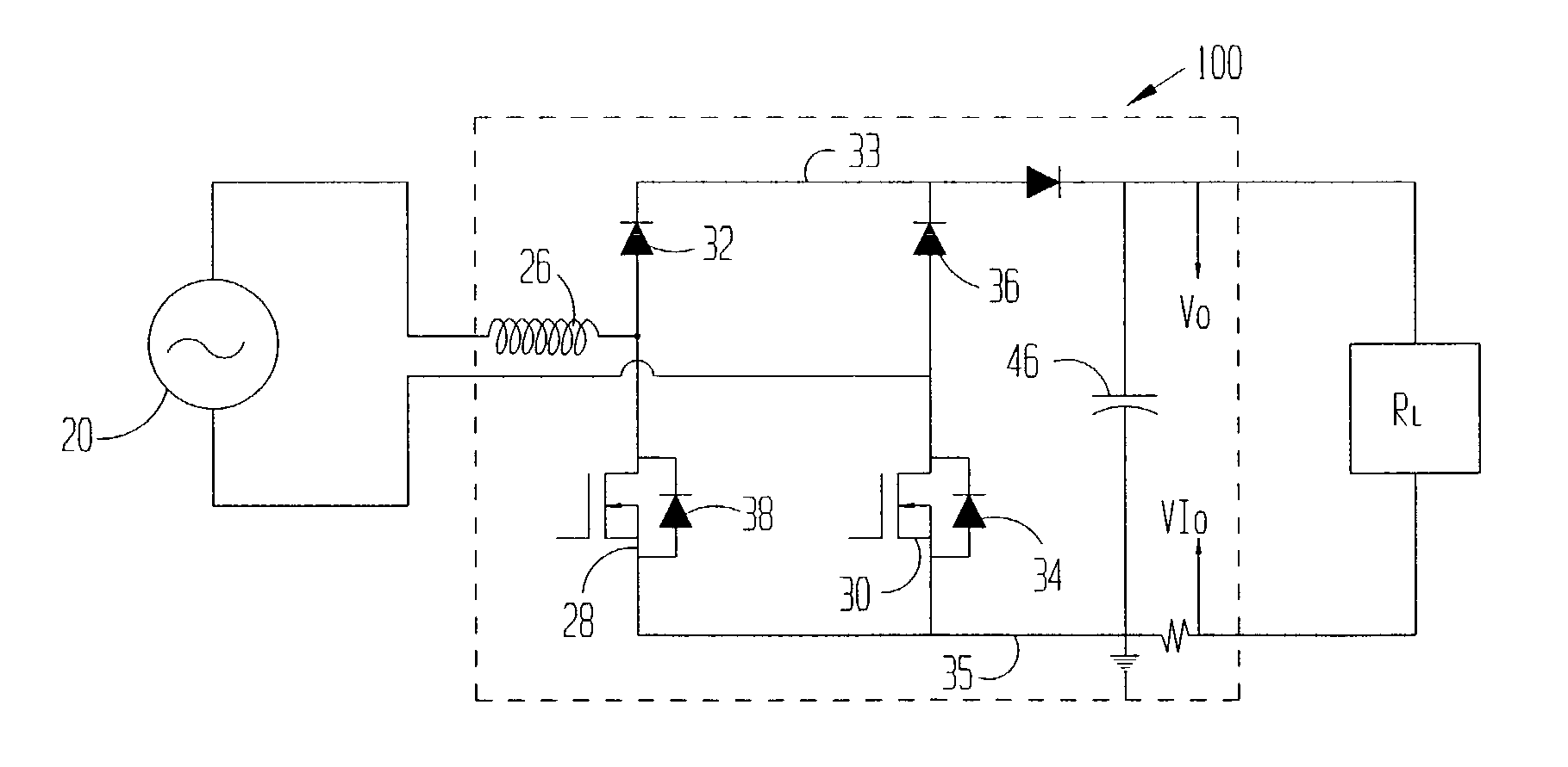
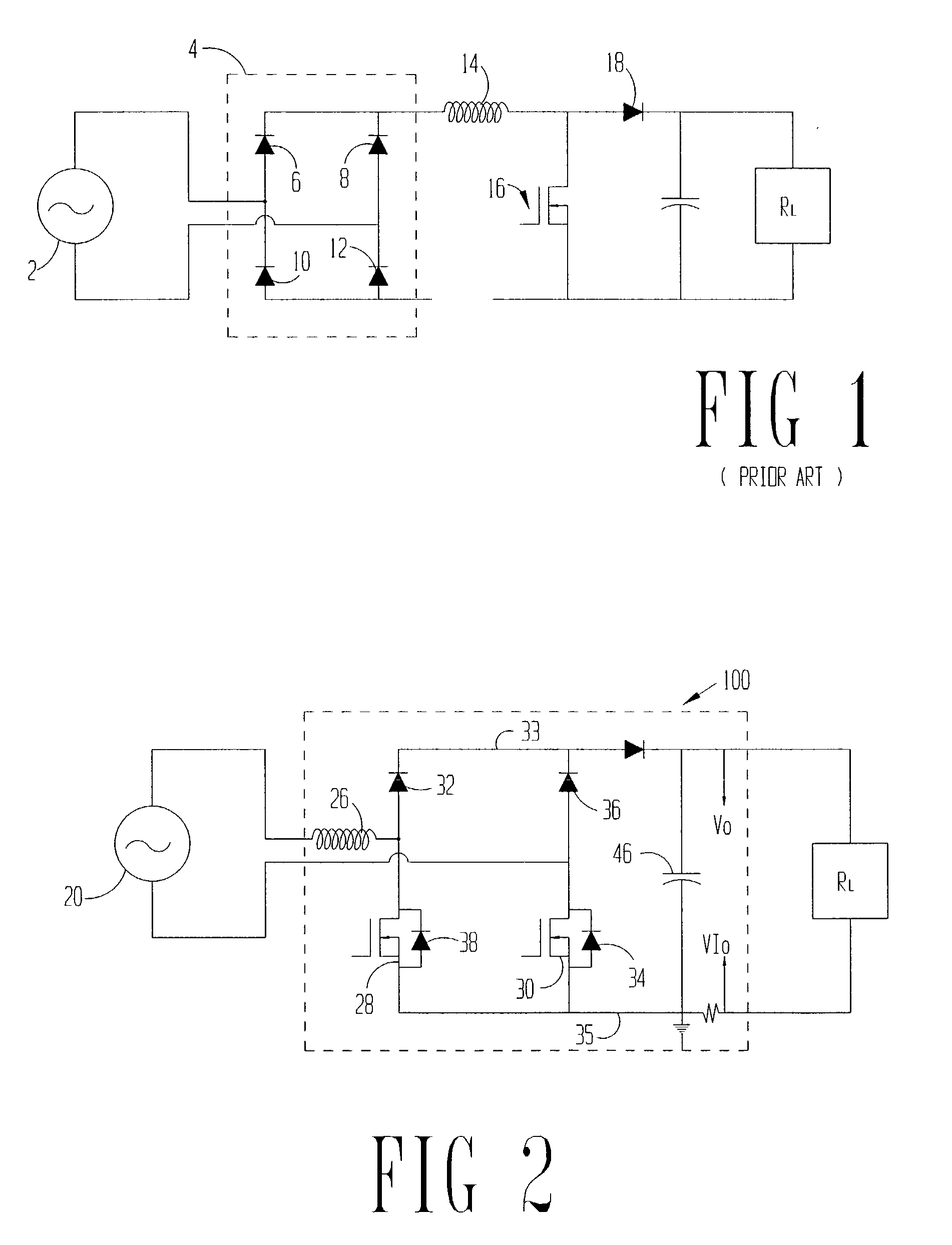
[0013] The problems noted above are solved in large part by an integrated bridge and boost circuit for a power conversion unit. More particularly, in the preferred embodiments, the inductor is coupled between the alternating current (AC) source and a rectifying bridge topology where at least two of the diodes are shunted with switch devices, which switch devices in the preferred embodiments are field effect transistors (FETs). Charging cycles of the inductor in either the positive or negative half cycle of the source voltage take place with current flowing through the inductor and back to the source through two FETs. The conduction power loss associated with the two FETs is significantly less than the power loss associated with the two diodes and boost switch experienced in the related art charging cycle. During the discharge cycle of the inductor, the current flow experiences the forward power loss associated with two power diodes, rather than the three diode forward power loss ass...


PUM


Abstract

The specification discloses an alternating current to direct current switching power supply, with power factor correction, and having an integrated rectifying bridge and boost circuit that results in the use of fewer power semiconductor devices in the rectification and boosting process. The use of fewer power semiconductor devices translates into a power supply with greater efficiency and / or smaller size. More particularly, the diodes in a rectifying bridge that typically conduct power back to the alternating current power source are paralleled by power MOSFETs, and the boost inductor is coupled between the source and the modified bridge. Charging of the boost inductor takes place through the power MOSFETs, resulting in only a two MOSFET power dissipation. Discharging of the boost inductor (and therefore supplying power not the load) takes place through two diodes, and therefore two forward power losses (as opposed to three diodes and three forward conduction losses associated in the related art). The reduction in internal power dissipation, therefore, results in smaller size and greater efficiency of the switching power supply.

Description

[0001] None.[0002] Not applicable.[0003] 1. Field of the Invention[0004] The preferred embodiments are directed generally to alternating current (AC) to direct current (DC) switching power supplies or power conversion units employing power factor correction circuitry. More particularly, the preferred embodiments are directed to AC to DC switching power supplies having an integrated rectifying bridge and boost control switch for power factor correction.[0005] 2. Background of the Invention[0006] FIG. 1 shows a schematic diagram of a switching power supply of the related art having an alternating current source 2 coupled to a full wave rectifier bridge 4 comprising four diodes 6, 8, 10 and 12. The bridge 4 converts the alternating current (AC) power signal from the source 2 into a direct current (DC) waveform having a ripple at twice the source frequency. In systems where the source 2 has a standard 120 volt root means square (rms) voltage operating at 60 hertz, the rectified waveform...

Claims


Application Information

Patent Timeline
IPC IPC(8): H02M7/219
CPCH02M1/4225H02M2001/0064H02M1/4233Y02B70/10H02M1/0064H02M1/0085
Inventor PRASAD, ALTURI R.NGUYEN, HAI N.SANTIN, JOSE A.REZA, MD. MASUD
Owner HEWLETT-PACKARD ENTERPRISE DEV LP
Why Eureka
Try Eureka