Ion source, ion implanting device, and manufacturing method of semiconductor devices

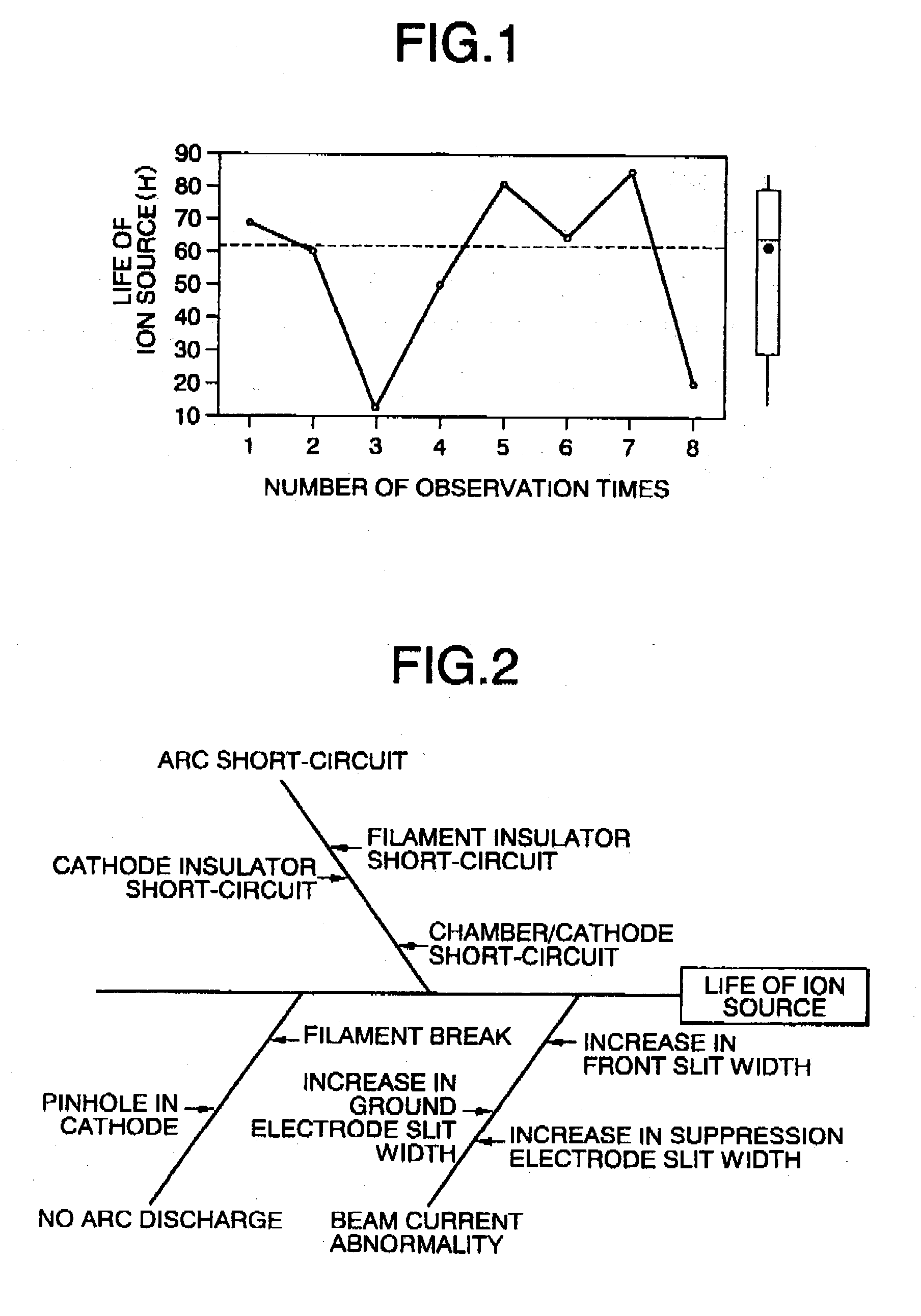
a manufacturing method and technology of semiconductor devices, applied in the direction of ion beam tubes, mechanical equipment, machines/engines, etc., can solve the problems of affecting productivity and production cost in manufacturing semiconductor devices, unable to perform desired operation, and remarkably short life of ion sources

Inactive Publication Date: 2004-04-08
KIOXIA CORP
View PDF6 Cites 9 Cited by
  • Summary
  • Abstract
  • Description
  • Claims
  • Application Information

AI Technical Summary

Problems solved by technology

This is because, when the ion implanting device is operated for use in manufacturing a semiconductor device and so on, the ion source is gradually deteriorated so that a desired operation is not performed.
It has been confirmed, however, that the life of the ion source is remarkably shortened when the ion implanting device is applied to such a low acceleration.
When the life of the ion source is thus shortened, it greatly influences productivity and production cost in manufacturing semiconductor devices.

Method used


Image

  • Ion source, ion implanting device, and manufacturing method of semiconductor devices
  • Ion source, ion implanting device, and manufacturing method of semiconductor devices
  • Ion source, ion implanting device, and manufacturing method of semiconductor devices

Examples


Embodiment Construction

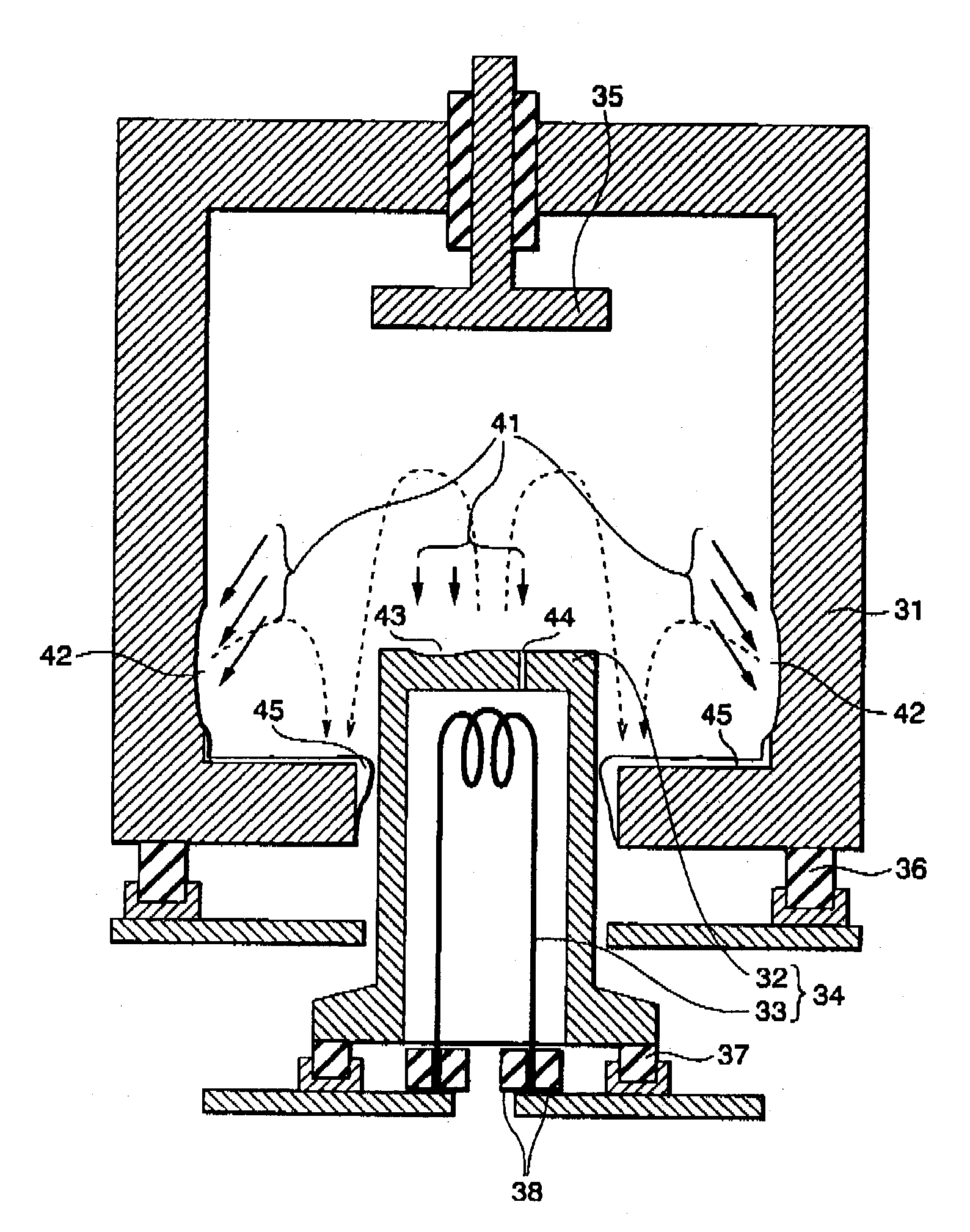
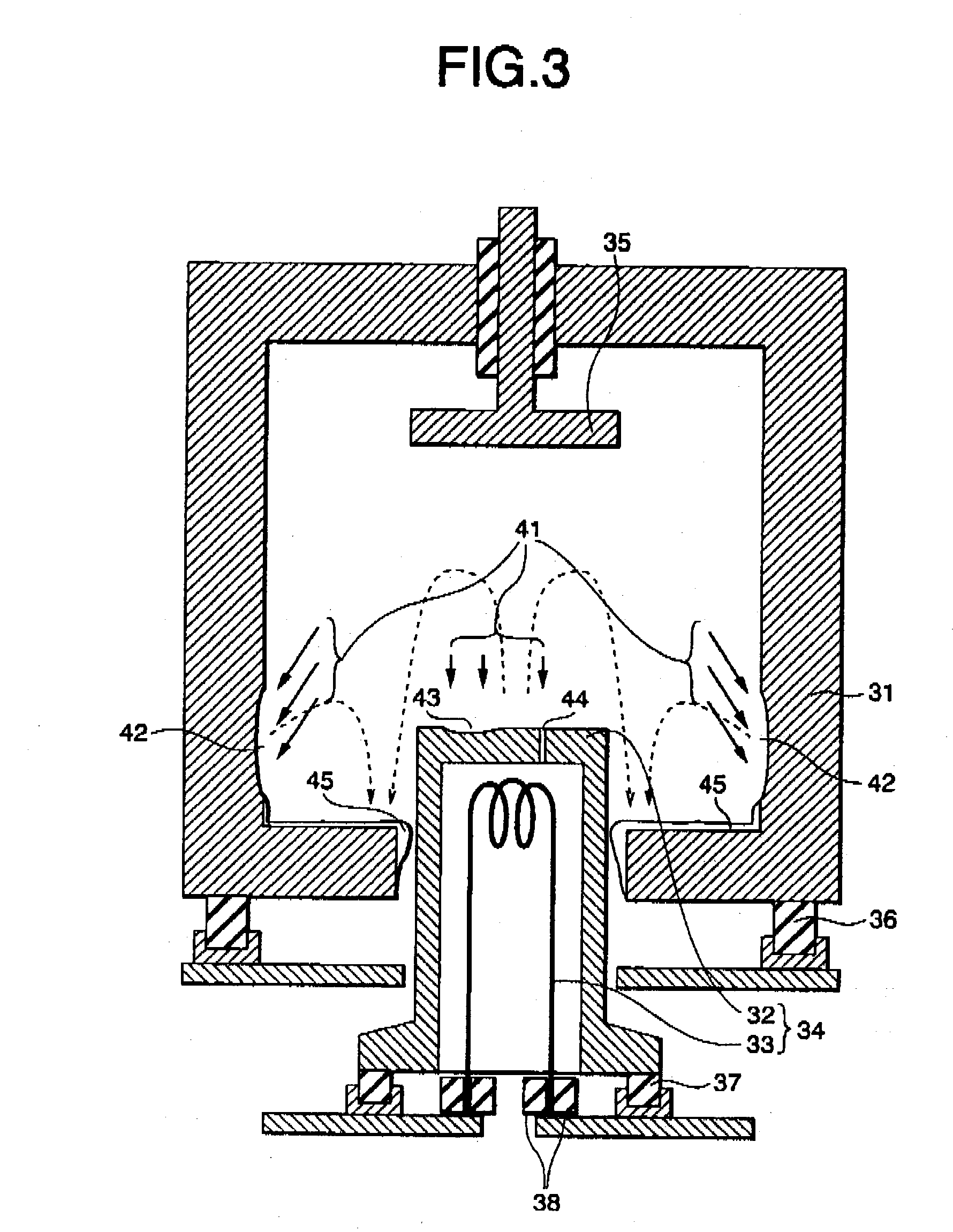
[0025] An ion source, an ion implanting device, and a method of manufacturing a semiconductor device according to an embodiment of the present invention use the following cathode as an internal structure of the ion source. Namely, this cathode is so structured that: i) it is insulatedly provided in a chamber and capable of discharging thermal electrons into the chamber; ii) it includes a cathode cap protruding into the chamber from an external side of an opening part which is formed to pass through from an external wall surface to an internal wall surface of the chamber and a filament disposed inside this cathode cap; and iii) the cathode cap and / or the filament is an alloy containing tungsten (w) as a major component and a predetermined metal element as a minor component.

[0026] According to the cathode as described above, the deterioration of the ion source is suppressed to elongate the life of the ion source. One of the causes of suppressing the deterioration of the ion source is ...


PUM

PropertyMeasurementUnit
inclination angleaaaaaaaaaa
energyaaaaaaaaaa

Abstract

This ion source includes a chamber having an internal wall surface and an external wall surface, and also includes a cathode, which is provided to be insulated from the chamber, capable of emitting thermal electrons into the chamber, and has a cathode cap protruding into the chamber from an external side of an opening part which is formed to pass through from the external wall surface to the internal wall surface of the chamber and a filament disposed inside the cathode cap, the cathode cap and/or the filament being an alloy containing tungsten (W) as a major component and a predetermined metal element as a minor component.

Description

CROSSREFERENCE TO RELATED APPLICATIONS[0001] This application is based upon and claims the benefit of priority from the prior Japanese Patent Application No. 2002-293887 filed on Oct. 7, 2002; the entire contents of which are incorporated herein by reference.[0002] 1. Field of the Invention[0003] The present invention relates to an ion source generating ions by plasmatizing a gas, an ion implanting device using such an ion source, and a manufacturing method of semiconductor devices using such an ion implanting device, and particularly, to the ion source, the ion implanting device, and the manufacturing method of semiconductor devices suitable for use in manufacturing micro-structured semiconductor devices.[0004] 2. Description of the Related Art[0005] In recent years, high integration of semiconductor devices used in electronic equipment, communication equipment, and so on advances more and more and integrated elements are becoming more micro-structured. It can be said that LSIs (la...

Claims


Application Information

Patent Timeline
Patent Type & Authority Applications(United States)
IPC IPC(8): C23C14/48H05H1/48H01J27/08H01J27/14H01J37/08H01J37/317H01L21/265
CPCH01J27/14H01J2237/31701H01J37/08
Inventor SUGURO, KYOICHI
Owner KIOXIA CORP
Why Eureka
Try Eureka