

Near-field photomask, near-field exposure apparatus using the photomask, dot pattern forming method using the exposure apparatus, and device manufactured using the method
a technology of near-field light and exposure apparatus, which is applied in the direction of photomechanical apparatus, printing, instruments, etc., can solve the problems of inability to solve, and inability to achieve the effect of solving the problem of solving the problem of inability to achieve the effect of solving the problem of inability to achieve the effect of reducing the intensity of the near-field light generated from the opening
- Summary
- Abstract
- Description
- Claims
- Application Information
AI Technical Summary
Problems solved by technology
Method used
Image

Examples
first embodiment
[0114] (First Embodiment)
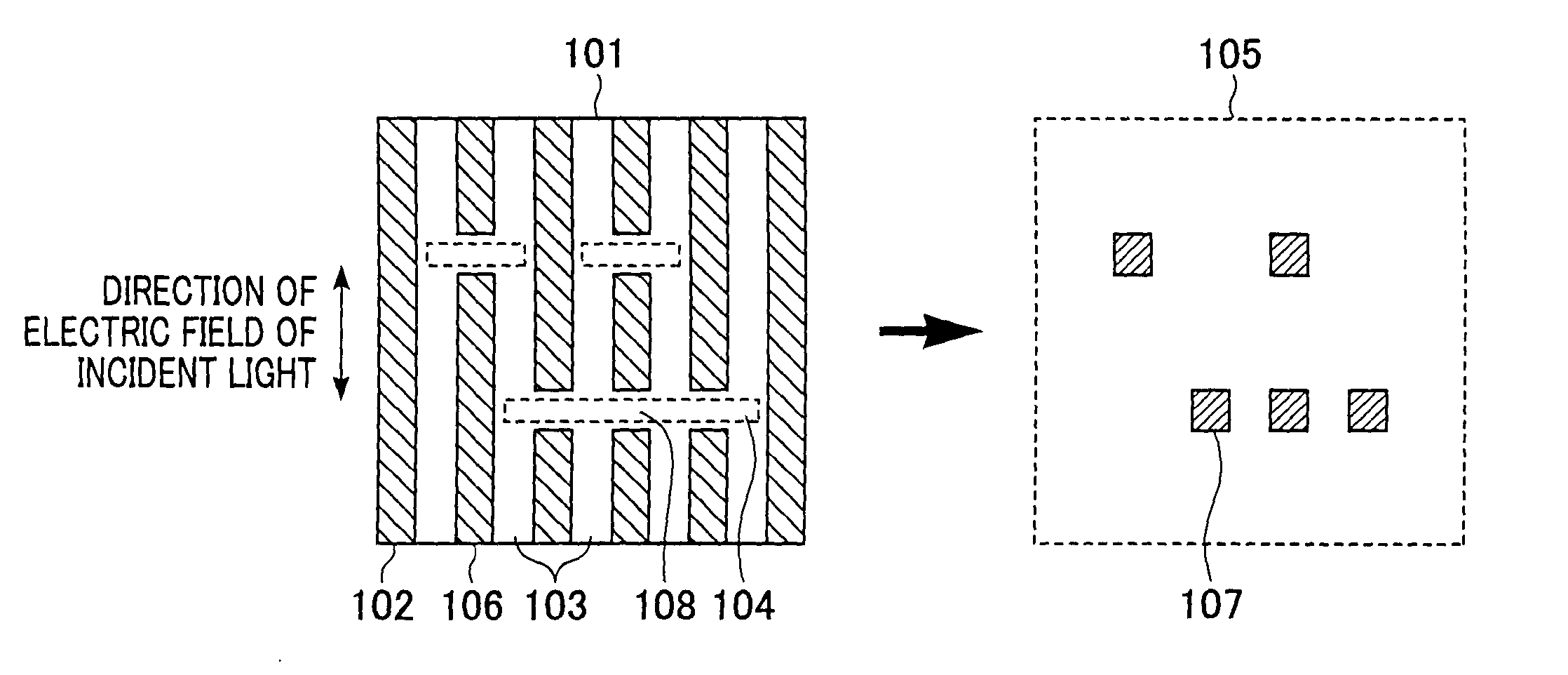
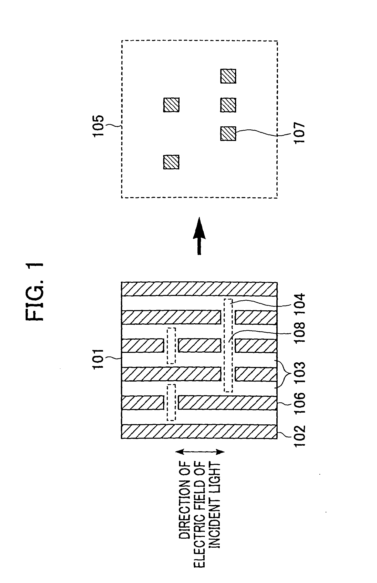
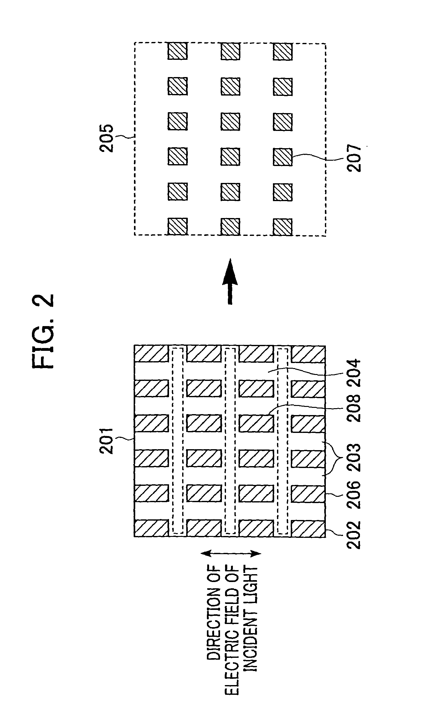
[0115] FIG. 2 shows a first embodiment of the opening pattern for the near-field photomask of the present invention.
[0116] Referring to FIG. 2, areas 208 where light shield portions 206 and second slit openings 204 in a near-field photomask 201 cross each other are arrayed in a rectangular lattice pattern. By exposing a photoresist with the use of the near-field photomask 201, a latent image pattern is formed as a pattern of dots arrayed in the form of a rectangular lattice as denoted by numeral 205.
[0117] The dimensions of the opening pattern formed in the near-field photomask 201 are, by way of example, as follows. A row of first slit opening 203 has a width of 40 nm, and the light shield portion 206 has a width of 20 nm. The second slit opening 204 has a width of 20 nm, the interval between adjacent two of a plurality of second slit openings 204 is 60 nm, and the crossed area 208 has a size of 20 nm.times.20 nm. In this case, the latent image pattern 205 ...
second embodiment
[0118] (Second Embodiment)
[0119] FIG. 3 shows a second embodiment of the opening pattern for the near-field photomask of the present invention.
[0120] Referring to FIG. 3, areas 308 where light shield portions 306 and second slit openings 304 in a near-field photomask 301 cross each other are arrayed in a triangular lattice pattern. By exposing a photoresist with the use of the near-field photomask 301, a latent image pattern is formed in the photoresist as a pattern of dots arrayed in the form of a triangular lattice as denoted by numeral 305.
[0121] The dimensions of the opening pattern formed in the near-field photomask 301 are, by way of example, as follows. A row of first slit opening 303 has a width of 40 nm, and the light shield portion 306 has a width of 20 nm. The second slit opening 304 has a width of 20 nm, the interval between adjacent two of a plurality of second slit openings 304 is 60 nm, and the crossed area 308 has a size of 20 nm.times.20 nm. In this case, the latent...
third embodiment
[0122] (Third Embodiment)
[0123] FIG. 4 shows a third embodiment of the opening pattern for the near-field photomask of the present invention.
[0124] Referring to FIG. 4, areas 408 where light shield portions 406 and second slit openings 404 in a near-field photomask 401 cross each other are arrayed in a hexagonal lattice pattern. By exposing a photoresist with the use of the near-field photomask 401, a latent image pattern is formed in the photoresist as a pattern of dots arrayed in the form of a hexagonal lattice as denoted by numeral 405.
[0125] The dimensions of the opening pattern formed in the near-field photomask 401 are, by way of example, as follows. A row of first slit opening 403 has a width of 40 nm, and the light shield portion 406 has a width of 20 nm. The second slit opening 404 has a width of 20 nm, the interval between adjacent two of a plurality of second slit openings 404 is 40 nm, and the crossed area 408 has a size of 20 nm.times.20 nm. In this case, the latent ima...
PUM
 Abstract
Description
Claims
Application Information