
Microfabrication of pattern imprinting

a micro-printing and pattern technology, applied in the field of micro-printing patterns, can solve the problems of consuming a vast amount of pattern-making time, limited degree of resolution achievable by photolithography, and ultimately limited minimum line width, and achieve the effect of simple method and low cos

Inactive Publication Date: 2006-10-03
EBARA CORP +1
View PDF13 Cites 8 Cited by
  • Summary
  • Abstract
  • Description
  • Claims
  • Application Information

AI Technical Summary

Benefits of technology

[0011]It is an object of the present invention to provide an optical imprinting apparatus and method for producing a two-dimensional pattern, having line widths less than the wavelength of an exposure light, economically using a simple method and a low cost device.
[0012]It is another object of the invention to provide an imprinting method for imprinting two dimensional micro patterns with high aspect ratio.

Problems solved by technology

The degree of resolution achievable by photolithography is limited by light diffraction effects, and the minimum line width is ultimately limited by the wavelength with respect to light.
However, in this technique, the proximity field can only be produced at the tip of the optical fiber opposite to the base, therefore, the exposed pattern is a point.
To apply this technique to the production of a two-dimensional pattern of some integrated circuit device, it is necessary to scan the tip in a pattern of the circuit, so that it not only consumes a vast amount pattern-making time but also leads to the need for a complex tip-driving apparatus.
Therefore, this technique is considered impractical.
However, the method requires that the incident beam be aligned with the inclination angle of a prism, and the optical system is necessarily complex.
Also, the exposure pattern section can only accept a small exposure area.
And, because the incident light is at an angle to the proximity field exposure pattern, the depth of imprinting is shallow, and because the exposed area increases quickly along the beam line, it is difficult to expose a structure having high aspect ratios on the photo-resist film.

Method used


Image

  • Microfabrication of pattern imprinting
  • Microfabrication of pattern imprinting
  • Microfabrication of pattern imprinting

Examples


Embodiment Construction

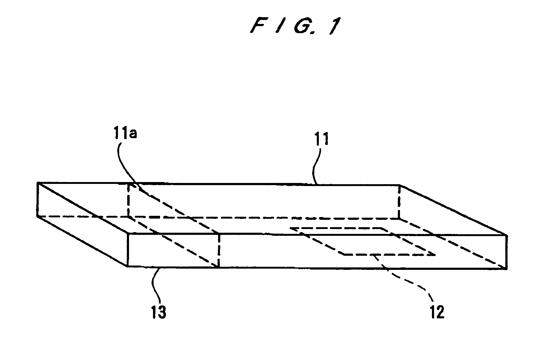
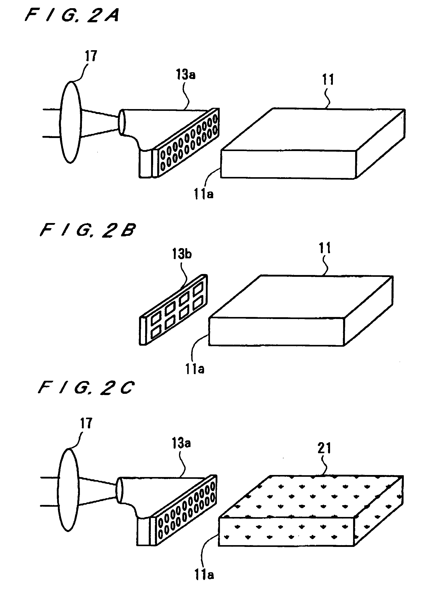
[0103]FIG. 1 shows an embodiment of a photo-driven imprinting apparatus. A proximity field exposure pattern (shortened to proximity pattern hereinbelow) 12 is fixed to a section of a waveguide 11. A light source 13 is connected to an input surface 11a of the waveguide 11, and a light input into the input surface 11a propagates through the waveguide 11. The waveguide 11 is a flat plate, and its upper and lower surfaces are treated so as to obtain total reflection between the two surfaces. For example, all the surfaces, excepting both sections of the input surface 11a and the proximity pattern 12, are coated with a metal film. The waveguide 11 is made of quartz glass or a light-transmissive material such as polyimide, and excepting the input / output surfaces, the surfaces are coated with a metal film such as Cr, Al, Ag or Au. Therefore, an incident light beam entering from the input surface 11a are trapped inside the transmissive material of the waveguide 11. Thus the waveguide 11 can ...


PUM


Abstract

An optical imprinting apparatus, and a method for producing a two-dimensional pattern, have line widths less than the wavelength of an exposure light. The evanescent (proximity) field effect is adopted to realize the apparatus and method. An optical imprinting apparatus comprises a container in which light is enclosed, an exposure-mask having a proximity field exposure pattern firmly fixed to a section of the container for exposing the exposure pattern on a photo-sensitive material through an evanescent field by the light enclosed therein; and a light source for supplying the light in the container.

Description

[0001]This is a Divisional Application of U.S. patent application Ser. No. 09 / 301,311, filed Apr. 29, 1999, now U.S. Pat. No. 6,671,034, issued Dec. 30, 2003.BACKGROUND OF THE INVENTION[0002]1. Field of the Invention[0003]The present invention relates to methods for imprinting micro-patterns, and relates in particular to a technique of evanescent (proximity)-field-assisted fabrication of two-dimensional micro-patterns of smaller dimensions than the wavelength of light.[0004]2. Description of the Related Art[0005]A typical example of fabrication techniques for making micro-circuit patterns on a semiconductor substrate is photolithography. In this technique, a photo-sensitive material (photo-resist) is coated on a substrate base, and a reduced image of a masking pattern containing micro-circuit patterns is projected on the base by optical means to expose the photo-resist material. The degree of resolution achievable by photolithography is limited by light diffraction effects, and the ...

Claims


Application Information

Patent Timeline
IPC IPC(8): G01F9/00G03C5/00G03F1/00G03F7/00G03F7/20
CPCB82Y10/00B82Y40/00G03F1/14G03F7/0002G03F7/2014G03F1/50
Inventor HATAKEYAMA, MASAHIROICHIKI, KATSUNORISATAKE, TOHRUHATAMURA, YOTARONAKAO, MASAYUKI
Owner EBARA CORP
Learn More