Method of manufacturing semiconductor device

a manufacturing method and semiconductor technology, applied in semiconductor devices, electrical equipment, electric discharge tubes, etc., can solve the problems of large surface area, inability to ensure reliability, and inability to remove impurities with the elapse of standing tim

Inactive Publication Date: 2004-04-29
SPANSION LLC
View PDF8 Cites 55 Cited by
  • Summary
  • Abstract
  • Description
  • Claims
  • Application Information

AI Technical Summary

Problems solved by technology

In manufacturing a semiconductor device, a cleaning process of a semiconductor substrate is prepared between a certain manufacturing process and a subsequent manufacturing process since adhesion of very small particles and a very small amount of impurities obstructs the realization of a high-performance, high-reliability semiconductor device.
However, when the insulation film is to be formed on the semiconductor substrate, the amount of impurities such as organic matter adhering to the the elapse of the standing time after the semiconductor substrate undergoes the aforesaid wet cleaning.
Conventionally, since a chemical oxide film formed at the time of the wet cleaning comprises a solution containing hydrochloric acid to which the impurities such as organic matter easily adhere, the impurities give rise to an adverse effect with the elapse of the standing time.
More specifically, when a gate oxide film or a tunnel oxide film embracing the aforesaid chemical oxide film is formed, there exists a problem that the adhesion of the impurities such as organic matter causes rapid insulation degradation of the oxide film with the elapse of the standing time between the wet cleaning to the formation of the oxide film so that reliability cannot be ensured.
This chemical oxide film which is formed using the solution containing hydrochrolic acid, however, has a large surface area due to irregularity caused on the surface thereof so that impurities such as organic matter easily adhere thereto.
Consequently, the impurities give rise to a significant adverse effect.
Therefore, it is possible to reduce the surface area thereof and not to allow the impurities such as organic matter to easily adhere thereto.

Method used


Image

  • Method of manufacturing semiconductor device
  • Method of manufacturing semiconductor device
  • Method of manufacturing semiconductor device

Examples


Embodiment Construction

is Applied

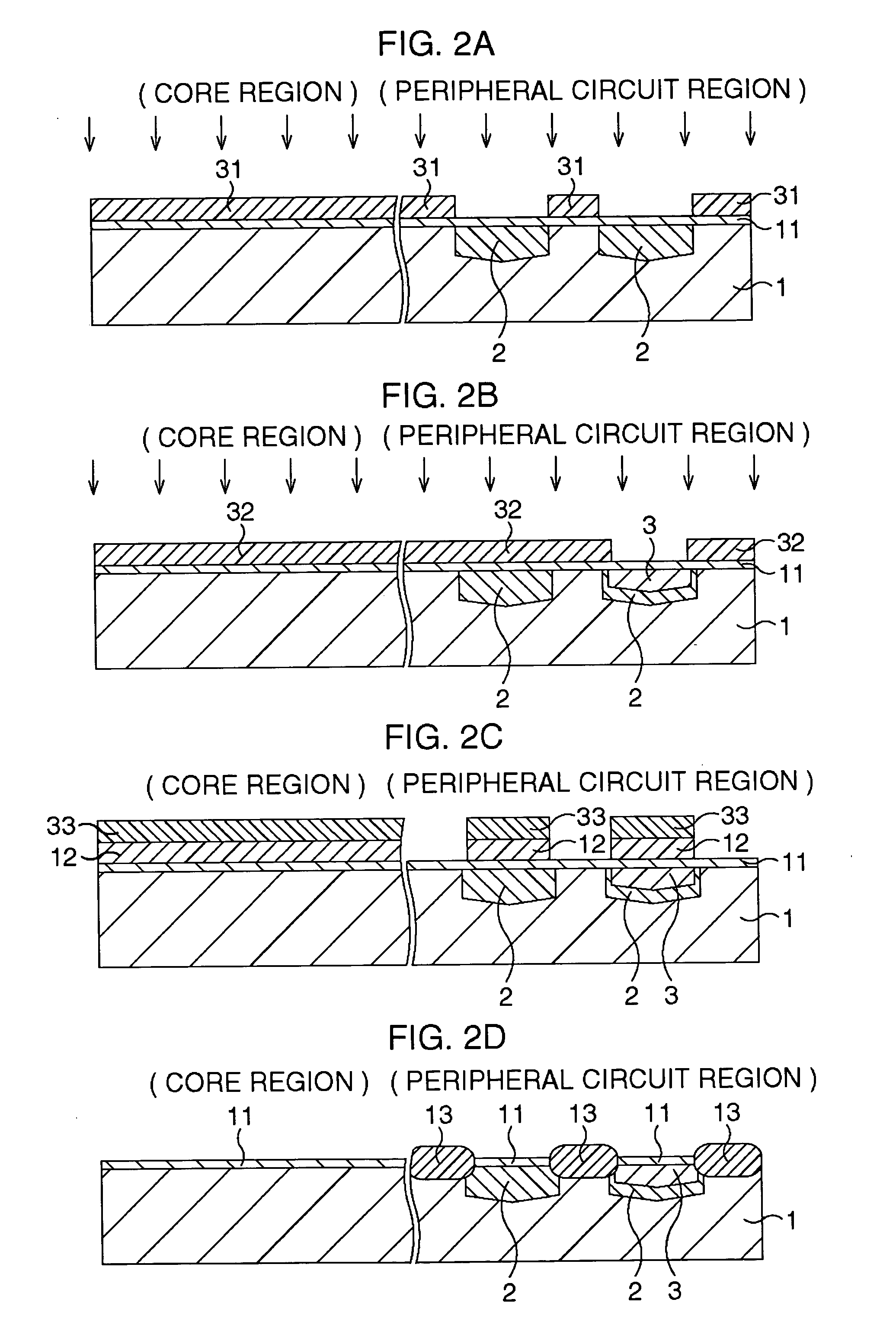
[0026] Next, an embodiment based on the basic structure of the method of manufacturing the semiconductor device in the present invention will be explained with reference to the attached drawings. In this embodiment, a semiconductor memory device having an embedded-bit-line-type SONOS structure will be disclosed as an example of the semiconductor device. This semiconductor memory device is so structured that SONOS transistors in a memory cell region (core region) are of a planer type and CMOS transistors are formed in a peripheral circuit region.

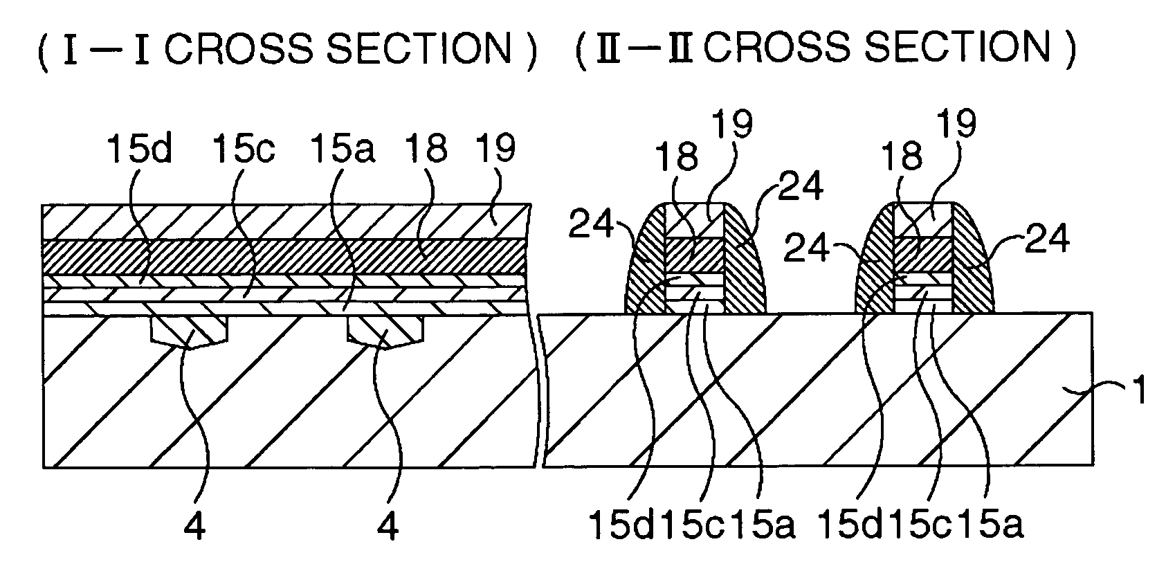
[0027] FIG. 2A to FIG. 5C are schematic cross sectional views showing a method of manufacturing a semiconductor memory device including embedded-bit-line-type SONOS transistors in this embodiment in the order of processes. Here, a view on the left side in each of the drawings shows a cross sectional view of the core region taken along the parallel line to a gate electrode (word line) and a view on the right side shows a cross sectio...


PUM


Abstract

A chemical oxide film formed on a semiconductor substrate is formed by wet cleaning using a strongly acidic solution so that the adhesion of impurities to the chemical oxide film can be reduced between a wet cleaning process and an insulation film forming process. This makes it possible to prevent insulation degradation of a gate insulation film when the gate insulation film embracing the chemical oxide film is formed in the insulation film forming process in which low-temperature processing is conducted.

Description

[0001] This application is based upon and claims the benefit of priority from the prior Japanese Patent Application No. 2002-273625, filed on Sep. 19, 2002, the entire contents of which are incorporated herein by reference.[0002] 1. Field of the Invention[0003] The present invention relates to a method of manufacturing a semiconductor device, and more particularly, to that suitable for use in forming a gate insulation film.[0004] 2. Description of the Related Art[0005] In manufacturing a semiconductor device, a cleaning process of a semiconductor substrate is prepared between a certain manufacturing process and a subsequent manufacturing process since adhesion of very small particles and a very small amount of impurities obstructs the realization of a high-performance, high-reliability semiconductor device. For this cleaning process, various cleaning methods are available, among which wet cleaning using a solution containing hydrochloric acid or the like is in the mainstream at pres...

Claims


Application Information

Patent Timeline
Patent Type & Authority Applications(United States)
IPC IPC(8): H01L21/314H01L21/8234H01L21/316H01L21/336H01L21/8238H01L21/8239H01L21/8246H01L21/8247H01L27/088H01L27/10H01L27/105H01L27/115H01L29/78H01L29/788H01L29/792
CPCH01J37/32192H01L21/3144H01L21/31654H01L21/823857H01L27/1052H01L27/105H01L27/115H01L27/11568H01L27/11573H01L21/823892H01L21/02233H01L21/02252H01L21/02247H10B99/00H10B69/00H10B43/30H10B43/40H01L21/18
Inventor NAKAMURA, MANABUNANSEI, HIROYUKISERA, KENTAROHIGASHI, MASAHIKOUTSUNO, YUKIHIROTAKAGI, HIDEOKAJITA, TATSUYA
Owner SPANSION LLC
Why Eureka
Try Eureka