Magnetoresistance device and method of fabricating the same
a technology of magnetoresistance and fabricated materials, applied in the direction of relays, magnetic bodies, substrate/intermediate layers, etc., can solve the problems of thermal stability, interdiffusion between hard and soft ferromagnetic layers, and reduction of coercive forces of free ferromagnetic layers
- Summary
- Abstract
- Description
- Claims
- Application Information
AI Technical Summary
Problems solved by technology
Method used
Image
Examples
first embodiment
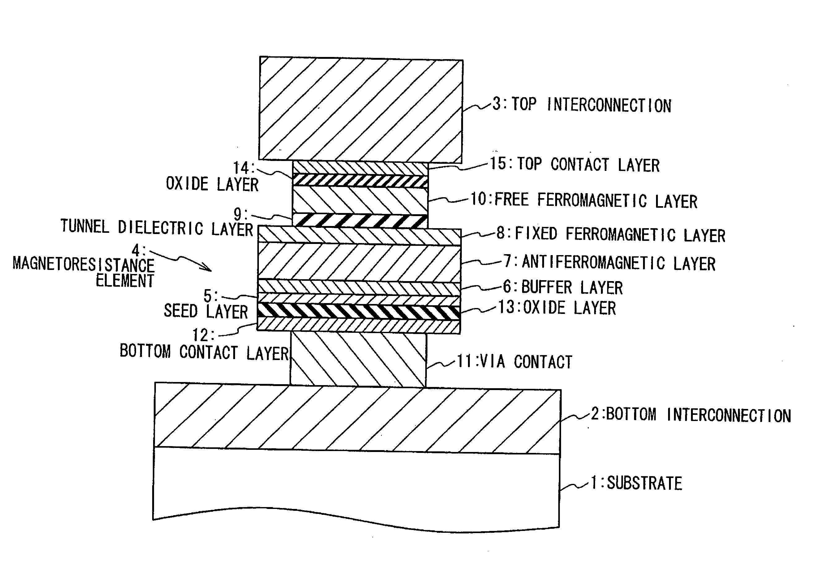
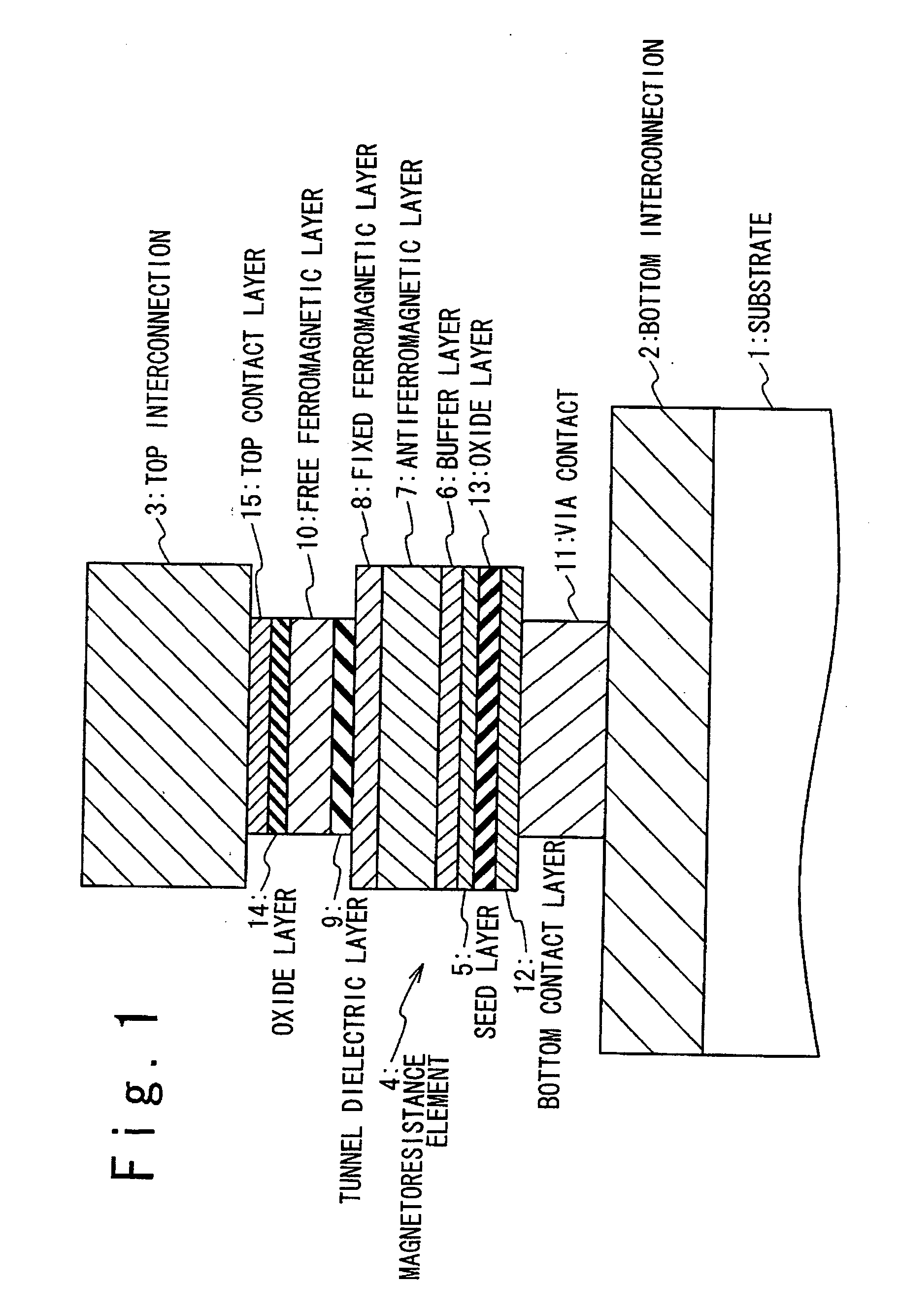
[0104] As shown in FIG. 1, one embodiment of the present invention addresses a cross-point cell type MRAM. In a first embodiment, bottom and top interconnections 2 and 3 are provided on an upper side of a substrate 1. The bottom and top interconnections 2 and 3 are formed of Al.sub.90Cu.sub.10.
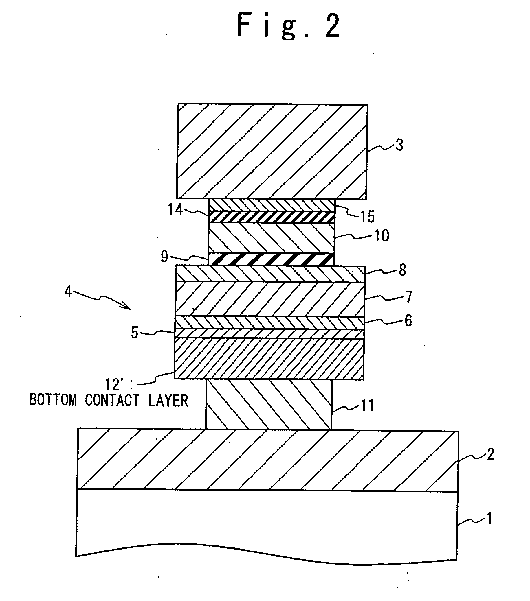
[0105] A magnetoresistance element 4, which functions as a memory cell of an MRAM, is disposed between the bottom and top interconnections 2 and 3. The magnetoresistance element 4 includes a seed layer 5, a buffer layer 6, an antiferromagnetic layer 7, a fixed ferromagnetic layer 8, a tunnel dielectric layer 9, and a free ferromagnetic layer 10. The fixed ferromagnetic layer 8, the tunnel dielectric layer 9, and the free ferromagnetic layer 10 within the magnetoresistance element 4 form a magnetic tunnel junction.
[0106] The fixed ferromagnetic layer 8 is formed of metal ferromagnetic alloy having a high spin polarization ratio, typically CoFe. CoFe alloy is relatively magnetically hard ferroma...
example 1 (
The Present Invention)
[0190] substrate / Ta(3 nm) / AlCu(50 nm) / Ta(3 nm) / Al.sub.2O.sub.3(1 nm) / Ta(3 nm) / Ni.sub.81Fe.sub.19(3 nm) / IrMn(10 nm) / Co.sub.90Fe.sub.10(6 nm) / AlO.sub.x(2 nm) / Co.sub.90Fe.sub.10(2.5 nm) / Ni.sub.81Fe.sub.19(7.5 nm) / Al.sub.2O.sub.3(1 nm) / Ta(5 nm) / AlCu(300 nm)
[0191] Comparative Example 1 corresponds with the structure shown in FIG. 1 with the oxide layers 13 and 14 omitted. Example 1 corresponds with the structure shown in FIG. 1, having the oxide layers 13 and 14 formed with Al.sub.2O.sub.3 of 1 nm in thickness. The AlCu layer of 50 nm in thickness corresponds with the bottom interconnection 2, while the AlCu layer of 300 nm in thickness corresponds with the top interconnection 3.
[0192] FIG. 19 illustrates changes in MR ratios of Comparative Example 1 and Example 1 depending on the thermal treatment temperature. Comparative Example 1 experience reduction in the MR ratio after the thermal treatment at the temperatures over 300.degree. C., while Example 1 is resistant ...
example 2 (
The Present Invention)
[0195] substrate / Ta(3 nm) / AlCu(50 nm) / Ta(3 nm) / Al.sub.2O.sub.3(1 nm) / Ta(3 nm) / Ni.sub.81Fe.sub.19(3 nm) / IrMn(10 nm) / Co.sub.90Fe.sub.10(4 nm), and
PUM
| Property | Measurement | Unit |
|---|---|---|
| thickness | aaaaa | aaaaa |
| thickness | aaaaa | aaaaa |
| thickness | aaaaa | aaaaa |
Abstract
Description
Claims
Application Information


