

Self boosting technique
a self-boosting and memory device technology, applied in the field of programming memory devices, can solve problems such as program disturbance, inadvertent programming, and low boosting potential
Inactive Publication Date: 2004-09-09
SANDISK TECH LLC
View PDF26 Cites 131 Cited by
- Summary
- Abstract
- Description
- Claims
- Application Information
AI Technical Summary
Benefits of technology
The present invention relates to programming memory devices, particularly flash memory devices, using a self-boosting technique. The technical effect of this invention is to provide a more efficient and reliable method for programming non-volatile memory cells, particularly in flash memory devices, which can use a NAND structure to achieve higher data storage capacity and reliability. The invention also includes a method for controlling the select lines and source line for programming the memory cells, as well as a method for connecting multiple NAND strings in a memory array.
Problems solved by technology
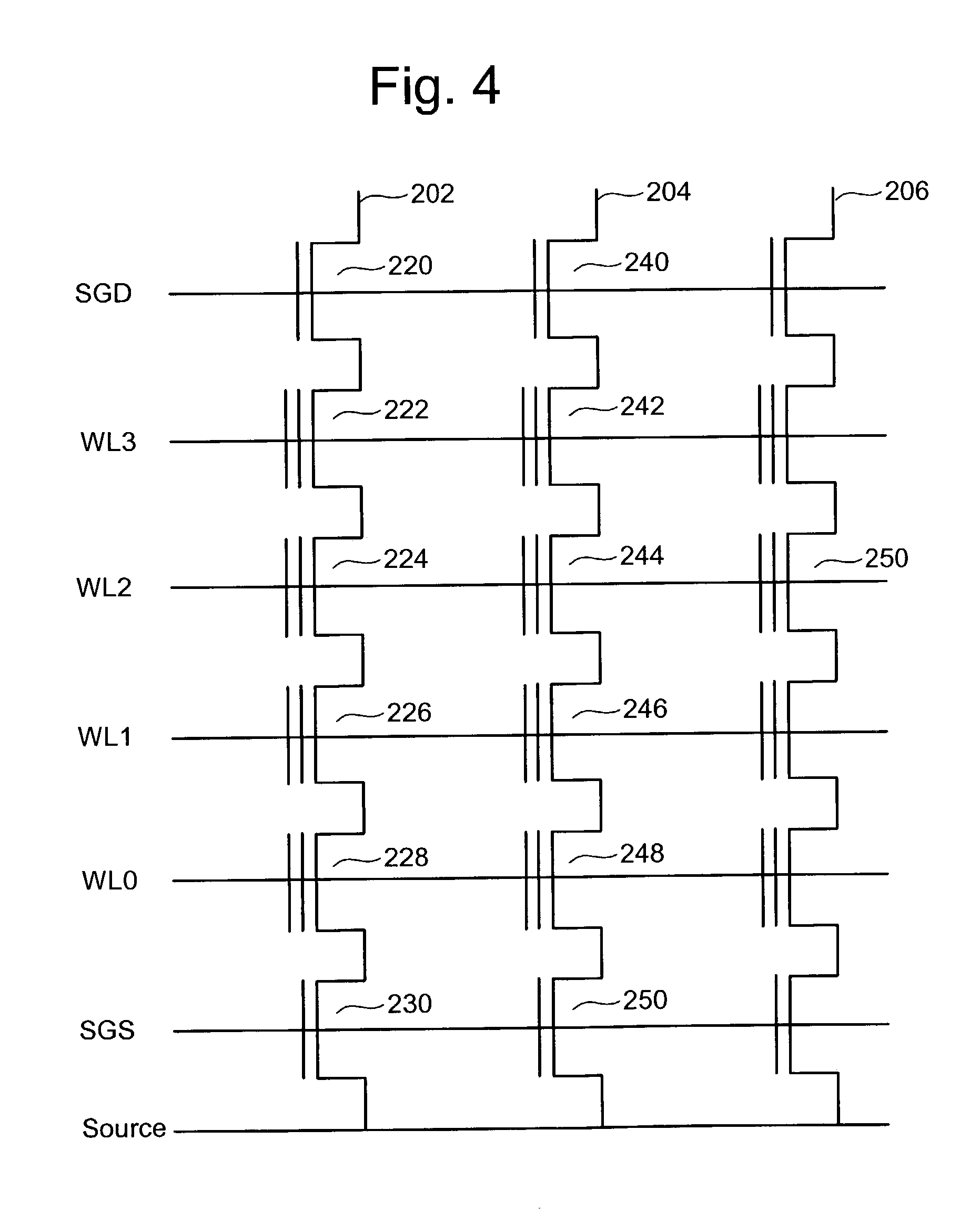
A problem arises when it's desired to program one cell on a word line without programming other cells connected to the same word line, for example, when it's desired to program cell 224 and not cell 244.
Because the program voltage is applied to all cells connected to a word line an unselected cell (a cell that is not to be programmed) on the word line, especially a cell adjacent to the cell selected for programming, may become inadvertently programmed.
Because of this negative charge on the floating gates, the boosting potential doesn't get high enough and there still may be program disturb on the last few word lines.
If Vpass is too low, boosting in the channel is insufficient to prevent program disturb.
While LSB and EASB provide an improvement over self boosting, they also present a problem that depends on whether the source side neighbor cell (cell 246 is the source side neighbor of cell 244) is programmed or erased.
GIDL will cause the boosted voltage to leak away prematurely, resulting in a programming error.
If the leakage current is high enough, the boosting potential in the channel region will go down and there can be program disturb.
Thus, the voltage in the boosted junction will drop quickly, causing program disturb.
Rather that string is operating in self boosting mode, and self boosting mode has the problems discussed above.
This scenario is most likely if other source side cells are programmed, which limits source side boosting.
This issue is most problematic with shorter channel lengths.
Programming cells with such small step increments in programming voltage results in increasing the programming time.
However, in practice, the erase process may result in some cells having negative threshold voltage below the predefined range.
Memory cells having a threshold voltage that is too low may not subsequently program properly.
One reason for the soft program process is that if the threshold voltages of a cell on the source side of the NAND string (with respect to the cell selected for programming) was very negative, then that source side may never turn off, which causes program disturb as described above.
Method used
View moreImage
Smart ImageViewing Examples

Examples
Embodiment Construction
has been presented for purposes of illustration and description. It is not intended to be exhaustive or to limit the invention to the precise form disclosed. Many modifications and variations are possible in light of the above teaching. The described embodiments were chosen in order to best explain the principles of the invention and its practical application to thereby enable others skilled in the art to best utilize the invention in various embodiments and with various modifications as are suited to the particular use contemplated. It is intended that the scope of the invention be defined by the claims appended hereto.
Login to View More PUM
 Abstract
A non-volatile semiconductor memory system (or other type of memory system) is programmed in a manner that avoids program disturb. In one embodiment that includes a flash memory system using a NAND architecture, program disturb is avoided by increasing the channel potential of the source side of the NAND string during the programming process. One exemplar implementation includes applying a voltage (e.g. Vdd) to the source contact and turning on the source side select transistor for the NAND sting corresponding to the cell being inhibited. Another implementation includes applying a pre-charging voltage to the unselected word lines of the NAND string corresponding to the cell being inhibited prior to applying the program voltage.
Description
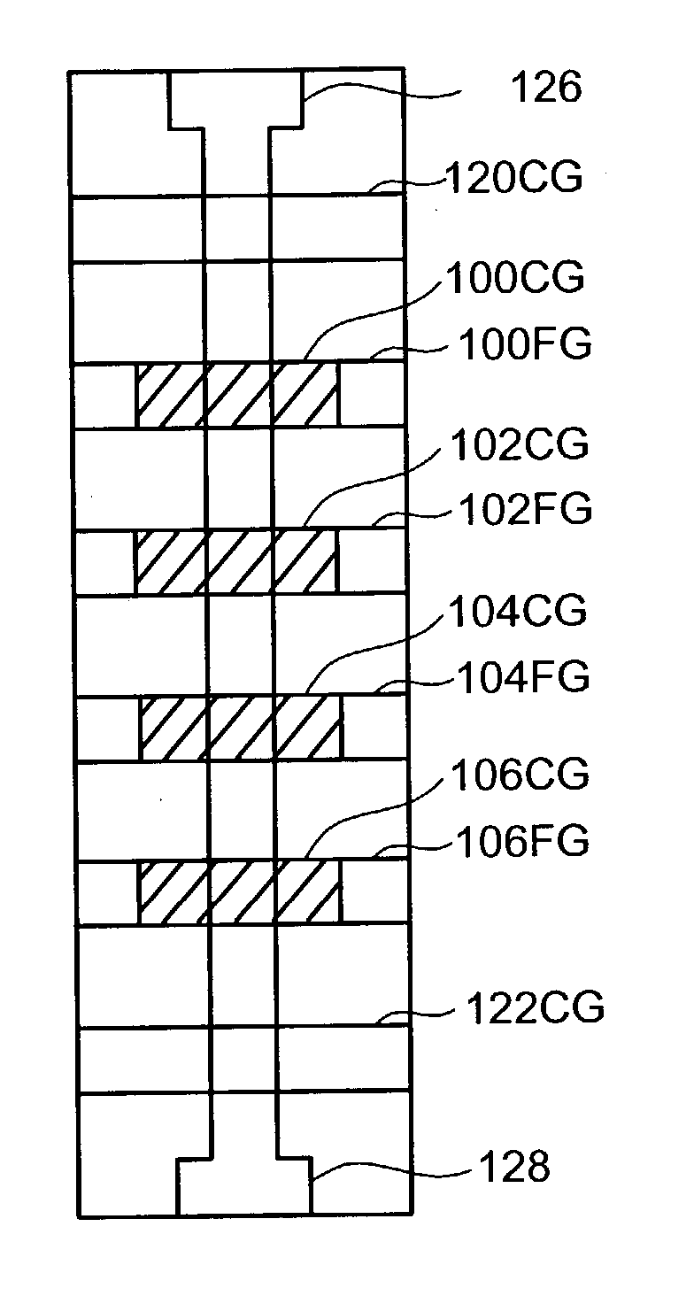
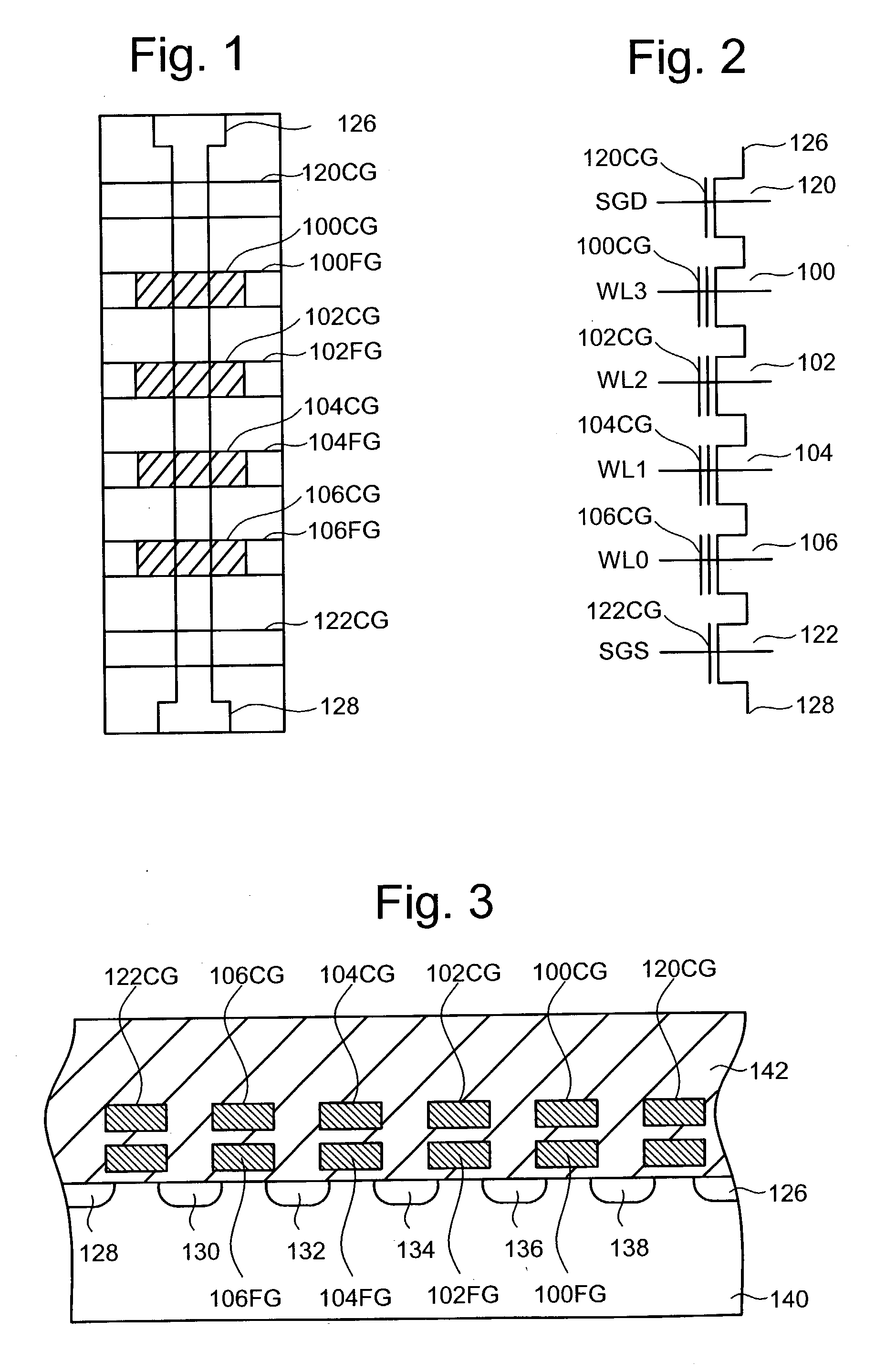
[0001] 1. Field of the Invention[0002] The present invention relates generally to technology for programming memory devices. In one embodiment, the present invention is directed to the programming of a non-volatile memory (e.g. a flash memory device) using a self boosting technique.[0003] 2. Description of the Related Art[0004] Semiconductor memory devices have become more popular for use in various electronic devices. For example, non-volatile semiconductor memory is used in cellular telephones, digital cameras, personal digital assistants, mobile computing devices, non-mobile computing devices and other devices. Electrical Erasable Programmable Read Only Memory (EEPROM) and flash memory are among the most popular non-volatile semiconductor memories.[0005] One example of a flash memory system uses the NAND structure, which includes arranging multiple transistors in series, sandwiched between two select gates. The transistors in series and the select gates are referred to as a NAND ...
Claims
Login to View More Application Information
Patent Timeline
 Patent Type & AuthorityApplications(United States)
IPC IPC(8): G11C11/34G11C11/56G11C16/04G11C16/10G11C16/34
CPCG11C11/5628G11C16/0483G11C16/3454G11C16/3418G11C16/10G11C16/12G11C16/30G11C16/3459
InventorLUTZE, JEFFREY W.CHEN, JIANLI, YANHIGASHITANI, MASAAKI
OwnerSANDISK TECH LLC