

Liquid crystal device and electronic equipment
a liquid crystal device and electronic equipment technology, applied in the direction of refrigerating machines, instruments, corrosion prevention, etc., can solve the problems of increasing cost, unstable domain structure, unstable disclination area,
- Summary
- Abstract
- Description
- Claims
- Application Information
AI Technical Summary
Benefits of technology
Problems solved by technology
Method used
Image

Examples
first exemplary embodiment
[0028] First Exemplary Embodiment
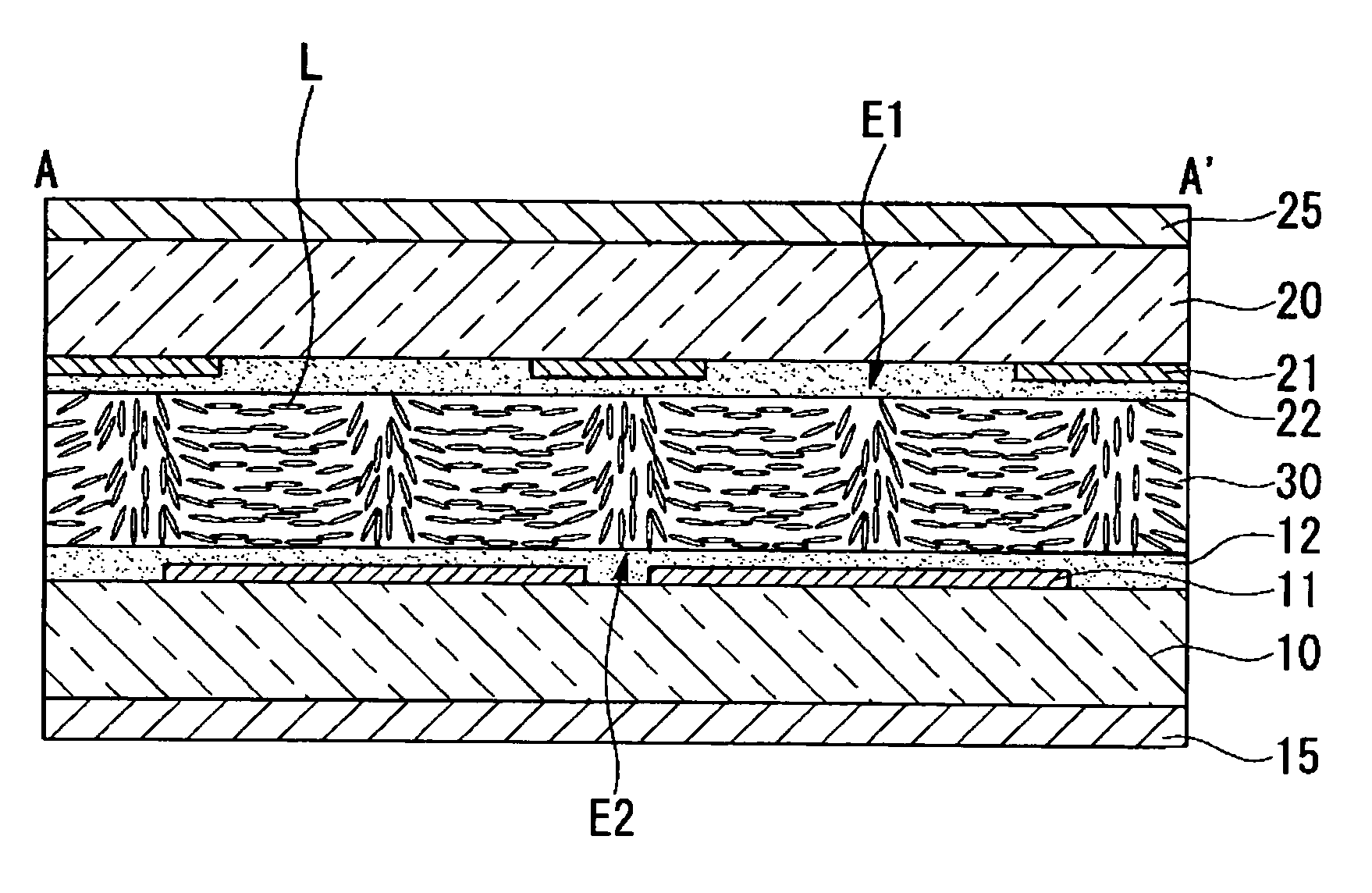
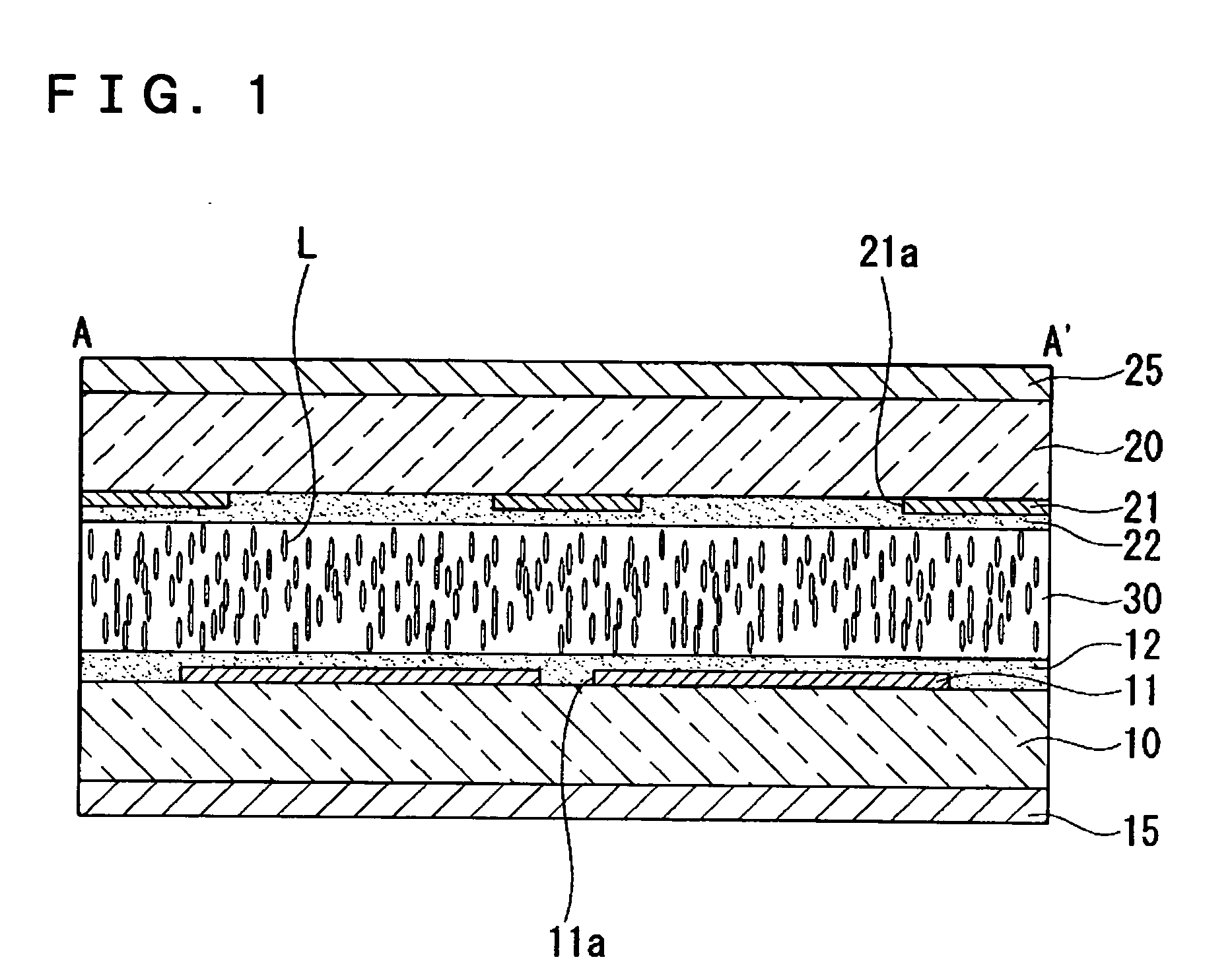
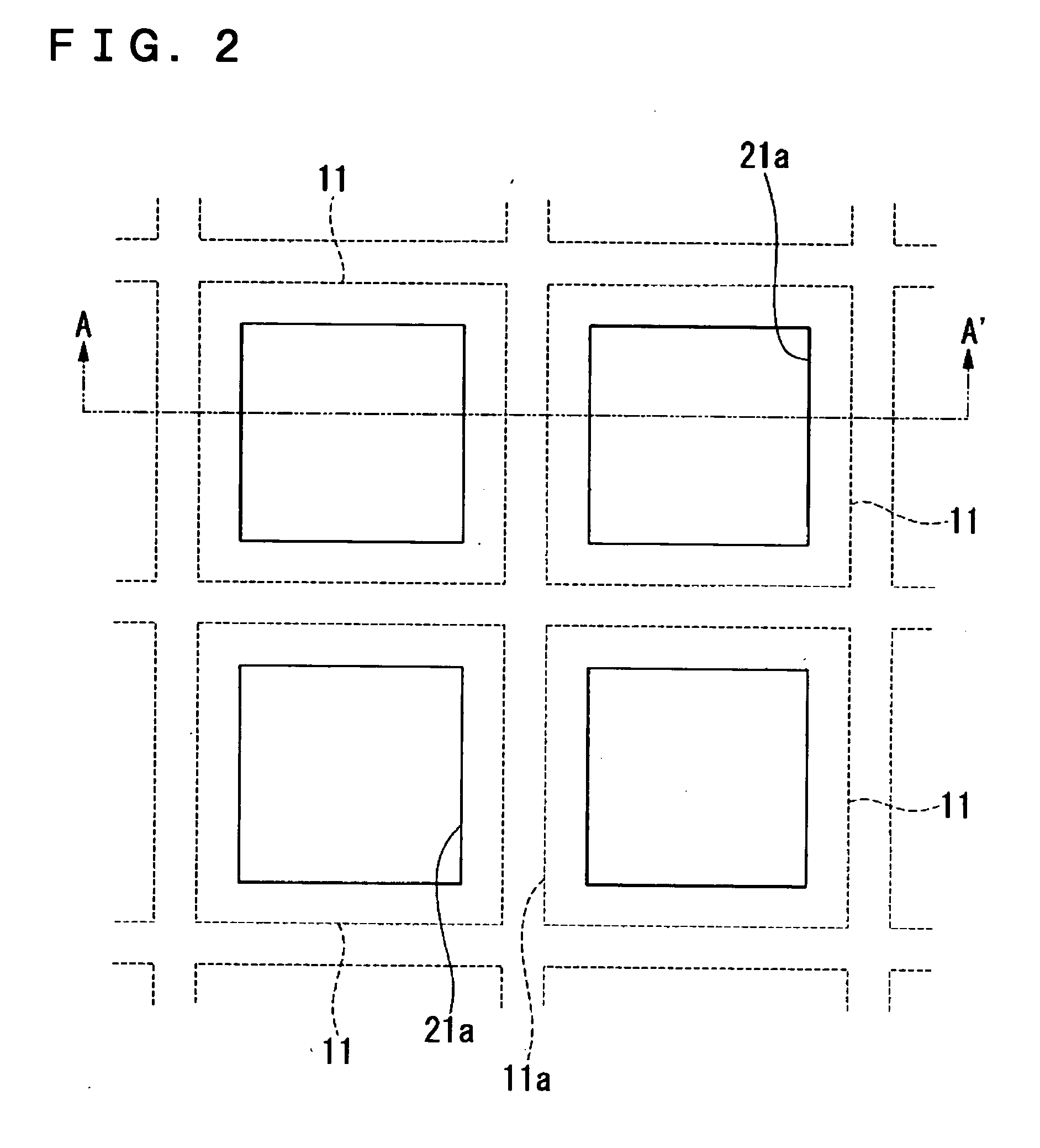
[0029] Referring now to FIG. 1 to FIG. 4, a liquid crystal device according to a first exemplary embodiment of the present invention will be described. FIG. 1 is a cross-sectional schematic showing a structure of the liquid crystal device according to the present exemplary embodiment. FIG. 2 is a schematic of a principal structure thereof when viewed from the side of the opposed substrate, FIG. 3 is a schematic showing a state of alignment of the liquid crystal when a voltage is applied. FIG. 4 is a schematic showing a state of alignment of the liquid crystal in one pixel. In these drawings, contraction scales of the layers or members are different from each other in order to make these layers or members recognizable in the drawings. In this specification, in each member constituting the liquid crystal device, the surface disposed on the side of the liquid crystal layer is referred to as "inner surface" and the opposite surface therefrom is referred ...
second exemplary embodiment
[0040] Second Exemplary Embodiment
[0041] Referring now to FIG. 5 and FIG. 6, the liquid crystal device according to a second exemplary embodiment of the present invention will be described. In the present embodiment, the same parts as in the aforementioned first exemplary embodiment are represented by the same reference numerals, and will not be described here.
[0042] The present exemplary embodiment is a modification in structure of the aforementioned first exemplary embodiment, in which the shape of the pixel electrode and the shape of the opening of the light shielding film are modified. In other words, as shown in FIG. 5, a pixel electrode 11' in the present exemplary embodiment has an octagonal shape with the corners of the pixel electrode 11 in the aforementioned first exemplary embodiment cut off, and the light shielding film is formed with octagonal openings 21a' correspondingly. The shape of the pixel electrode 11' and the shape of the openings of the light shielding film ma...
third exemplary embodiment
[0044] Third Exemplary Embodiment
[0045] Referring now to FIG. 7, the liquid crystal device according to a third exemplary embodiment of the present invention will be described. In the present exemplary embodiment, the same parts as in the aforementioned first exemplary embodiment are represented by the same reference numerals and will not be described here.
[0046] In the present exemplary embodiment of the invention, chiral material is added to a liquid crystal layer 30'. Hence alignment of the liquid crystal molecules L can be controlled more stably. In the liquid crystal device of a homeotropic alignment type described above, the liquid crystal molecules L fall down in the state of being twisted in predetermined directions when a voltage is applied. The twisting directions are not constant, but are unstable. Hence the twisting directions of the liquid crystal molecules are random among different pixels, although the twisting directions are the same in the same pixel. When the plura...
PUM
 Abstract
Description
Claims
Application Information