Single-electrode push-pull configuration for semiconductor PIN modulators

a single-electrode push-pull configuration and modulator technology, applied in the direction of semiconductor devices, instruments, optics, etc., can solve the problems of no cpw structure compatible with the design of a semiconductor based mzm, and achieve the effect of reducing the rf drive voltage 2.times

Inactive Publication Date: 2004-10-14
NORTHROP GRUMAN CORP
View PDF1 Cites 16 Cited by
  • Summary
  • Abstract
  • Description
  • Claims
  • Application Information

AI Technical Summary

Problems solved by technology

However, this technique has the disadvantage of requiring broadband power splitters that must maintain strict phase control over the frequency band of interest.
However, to date, no CPW structure compatible with the design of a semiconductor based MZM have been implemented to realize a 2.times. reduction in RF drive voltage.

Method used


Image

  • Single-electrode push-pull configuration for semiconductor PIN modulators
  • Single-electrode push-pull configuration for semiconductor PIN modulators

Examples


Embodiment Construction

[0014] The following discussion of the embodiments of the invention directed to a single-electrode, push-pull semiconductor PIN MZM is merely exemplary in nature, and is in no way intended to limit the invention or its applications or uses.

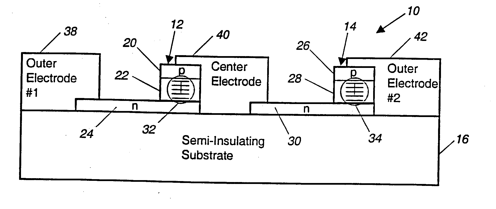
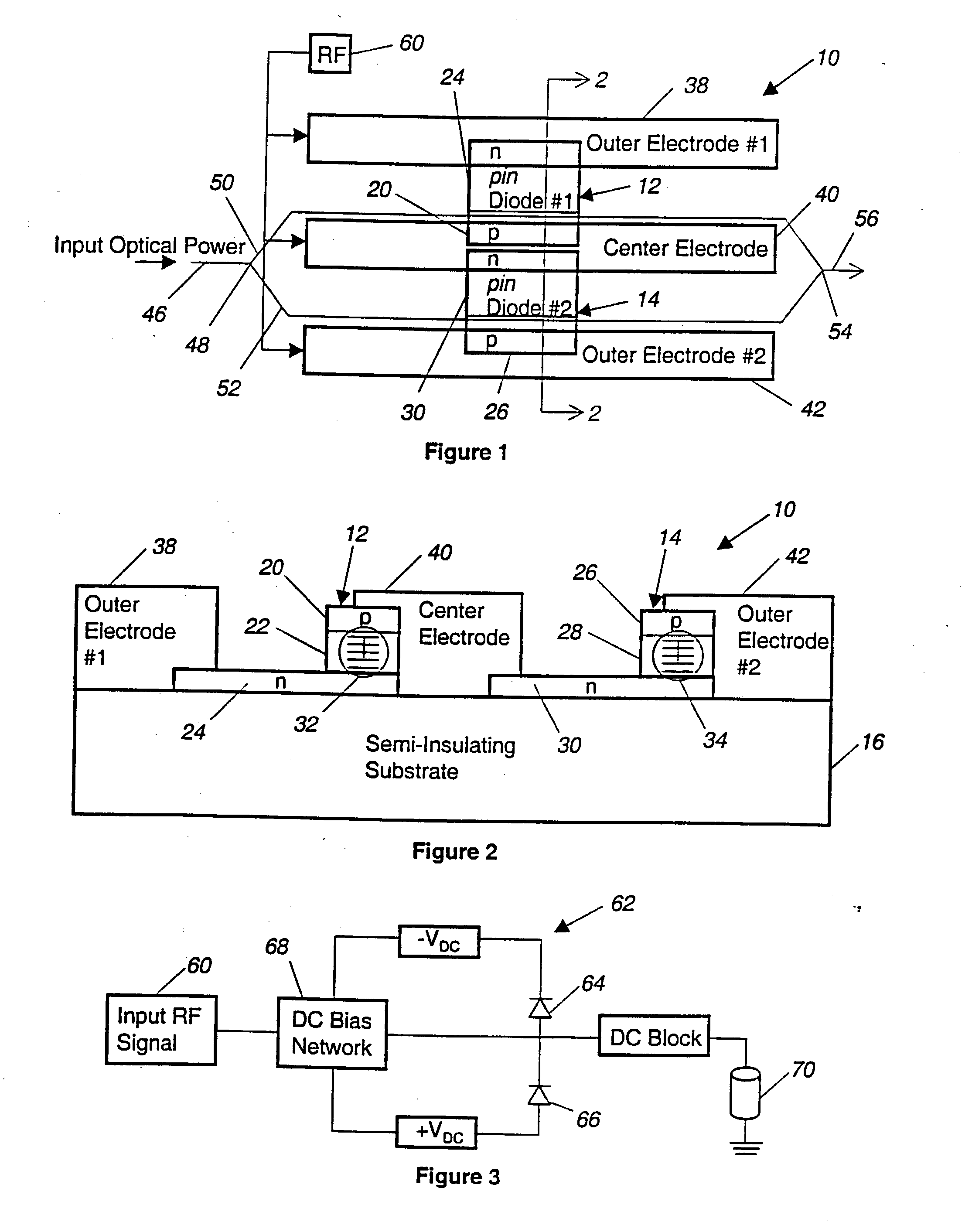
[0015] FIG. 1 is a top view and FIG. 2 is a cross-sectional view through line 2-2 in FIG. 1 of a semiconductor PIN Mach-Zehnder modulator 10. The modulator 10 includes a first PIN device 12 and a second PIN device 14 spaced apart from each other and formed on a semi-insulating substrate 16. The PIN devices 12 and 14 are conventional semiconductor devices, and the substrate 16 and the device layers of the PIN devices 12 and 14 can be any suitable semiconductor material, such as InP, for the purposes described herein. The PIN device 12 includes a P-type layer 20, an intrinsic layer 22 and an N-type layer 24, and the PIN device 14 includes a P-type layer 26, an intrinsic layer 28 and an N-type layer 30. The intrinsic layer 22 defines an active wavegu...


PUM

PropertyMeasurementUnit
optical index of refractionaaaaaaaaaa
index of refractionaaaaaaaaaa
DC bias voltageaaaaaaaaaa

Abstract

A single-electrode, push-pull semiconductor PIN Mach-Zehnder modulator (10) that includes first and second PIN devices (12, 14) on a substrate (16). Intrinsic layers (22, 28) of the devices (12, 14) are the active regions of two arms (50, 52) of a Mach-Zehnder interferometer. An outer electrode (38) is connected to the N layer (24) of the first PIN device (12) and a center electrode (40) is connected to the P layer (20) of the first PIN device (12). An outer electrode (42) is connected to the P layer (26) of the second PIN device (14) and the center electrode (40) is connected to the N layer (30) of the second PIN device (14). An RF modulation signal biases the PIN devices (12, 14) in opposite directions and causes the index refraction of the intrinsic layers (22, 28) to change in opposite directions to give a push-pull modulation effect.

Description

[0001] 1. Field of the Invention[0002] This invention relates generally to a semiconductor PIN Mach-Zehnder modulator and, more particularly, to a semiconductor PIN Mach-Zehnder modulator employing a single-electrode push-pull configuration.[0003] 2. Discussion of the Related Art[0004] Optical modulators are known in the art that use an electrical signal to frequency modulate an optical signal to impress information thereon. Optical modulators of this type that operate with low modulation voltages are needed in analog photonic link applications to improve link gain and noise figure. One class of modulators that operate at low modulation voltages are semiconductor modulators that employ PIN semiconductor devices where the optical wave propagates down an optical waveguide that includes an active region contained within the intrinsic layer in the device. An RF signal is applied to electrodes in contact with the P and N layers of the device to provide the modulation voltage across the i...

Claims


Application Information

Patent Timeline
Patent Type & Authority Applications(United States)
IPC IPC(8): G02F1/025G02F1/21G02F1/225H01S5/50
CPCG02F1/2257G02F2001/212G02F2201/126G02F1/212
Inventor SCOTT, DAVID C.VANG, TIMOTHY A.WANG, WENSHENKUNKEE, ELIZABETH T.
Owner NORTHROP GRUMAN CORP
Why Eureka
Try Eureka