Beam homogenizer, laser irradiation apparatus, and method for manufacturing semiconductor device

a laser irradiation and laser irradiation technology, applied in the direction of instruments, optical elements, optics, etc., can solve the problems of lowering the usability of energy and inhomogeneity of energy distribution

Inactive Publication Date: 2004-10-28
SEMICON ENERGY LAB CO LTD
View PDF52 Cites 52 Cited by
  • Summary
  • Abstract
  • Description
  • Claims
  • Application Information

AI Technical Summary

Problems solved by technology

The laser beam reaching the surface to be irradiated without being influenced by the cylindrical lens may cause inhomogeneity of the energy distribution of the rectangular beam spot on the irradiated surface.
This causes the lowering of t

Method used


Image

  • Beam homogenizer, laser irradiation apparatus, and method for manufacturing semiconductor device
  • Beam homogenizer, laser irradiation apparatus, and method for manufacturing semiconductor device
  • Beam homogenizer, laser irradiation apparatus, and method for manufacturing semiconductor device

Examples


embodiment 1

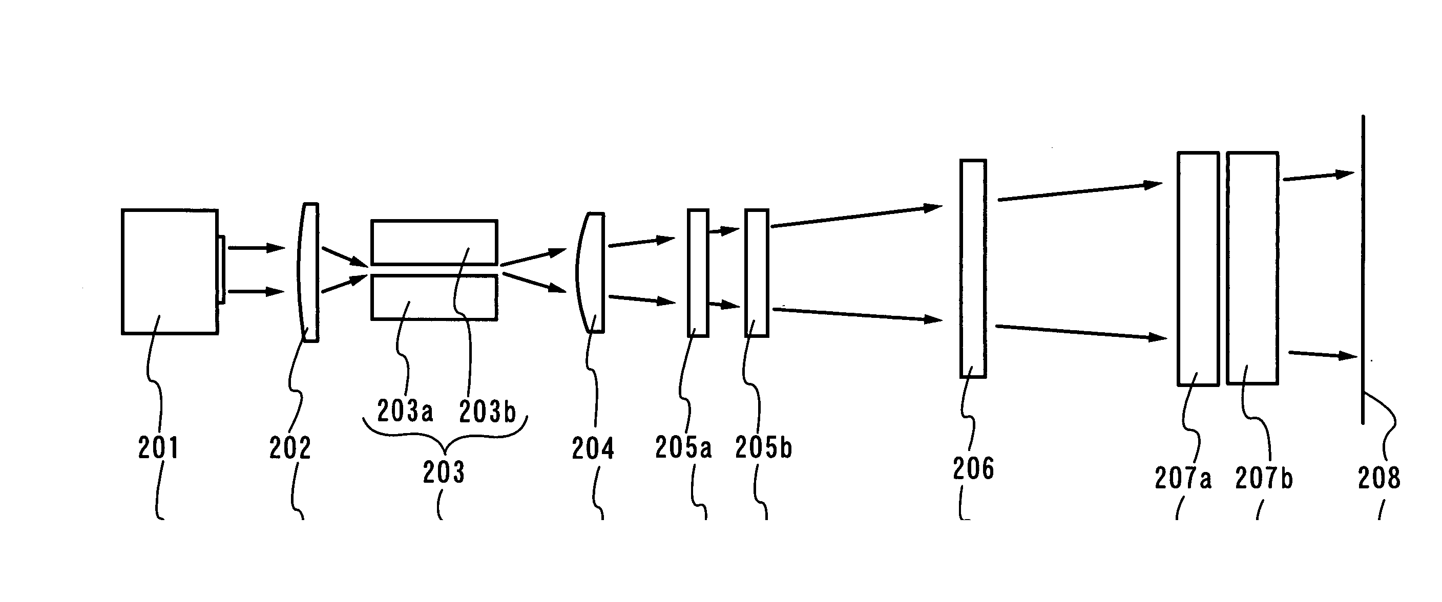
[0075] FIGS. 3A and 3B show an example of the optical system including an optical waveguide to be explained in this embodiment. A light pipe can be used as the optical waveguide. First, a top view of FIG. 3A is explained. A laser beam emitted from a laser oscillator 301 is propagated to the direction indicated by an arrow in FIGS. 3A and 3B. In the top view of FIG. 3A, the direction perpendicular to the paper is the direction of the minor axis of the rectangular beam spot.

[0076] Initially, the laser beam is expanded by spherical lenses 302a and 302b. When a laser oscillator 301 emits a sufficiently large beam spot, such a structure is not necessary. It is noted that the optical system for expanding the shape of the beam spot such as the spherical lenses 302a and 302b is generally referred to as a beam expander.

[0077] The laser beam expanded by the beam expander is focused in the direction of the major axis of the rectangular beam spot through a cylindrical lens 303 having a thicknes...

embodiment 2

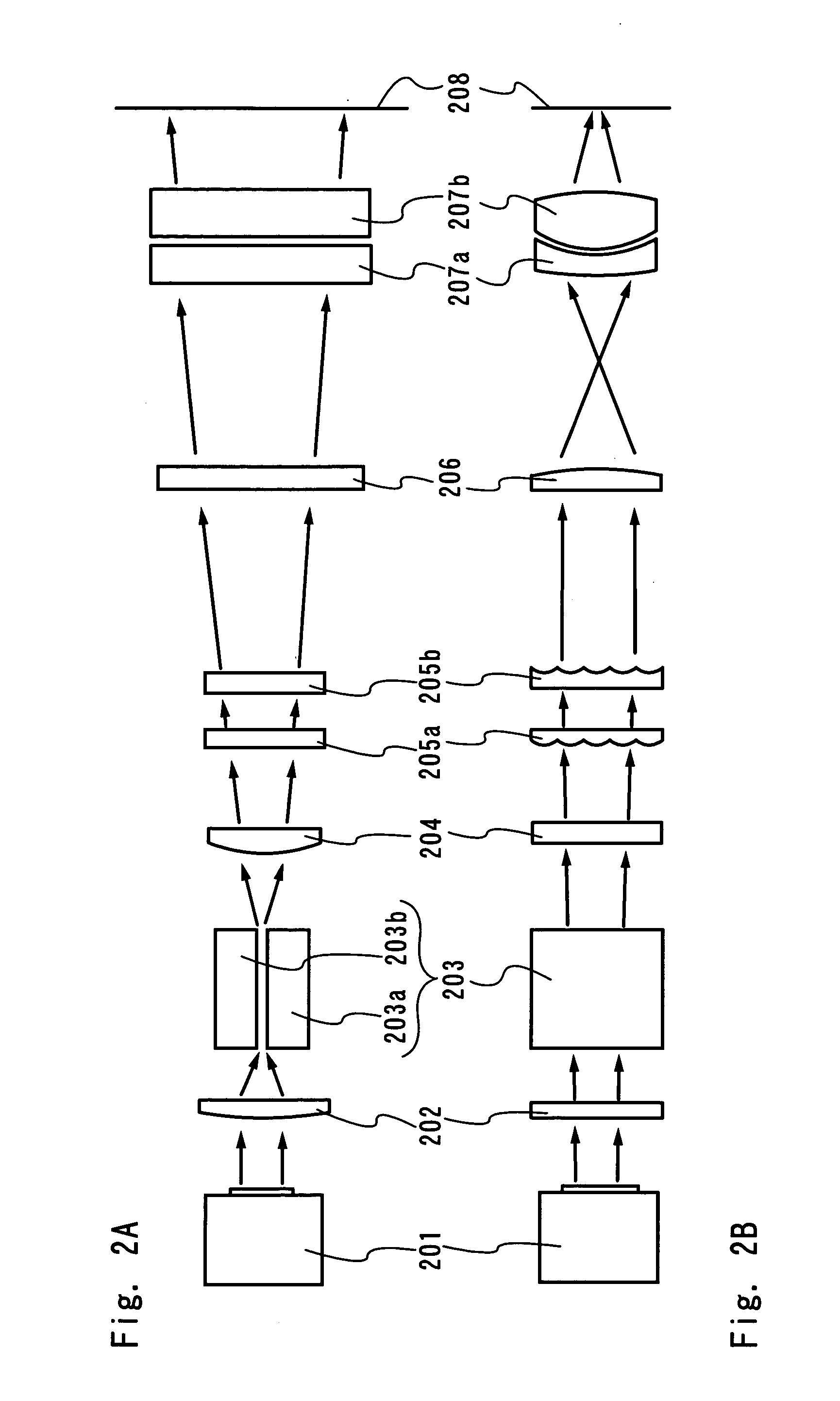
[0086] This embodiment shows an example of the different optical system from that described in the embodiment mode. FIGS. 5A and 5B show the example of the optical system to be explained in this embodiment. In addition, a light pipe can be used as the optical waveguide. In addition, in FIGS. 5A and 5B, the same part as that in FIGS. 3A and 3B is shown with the same reference numeral.

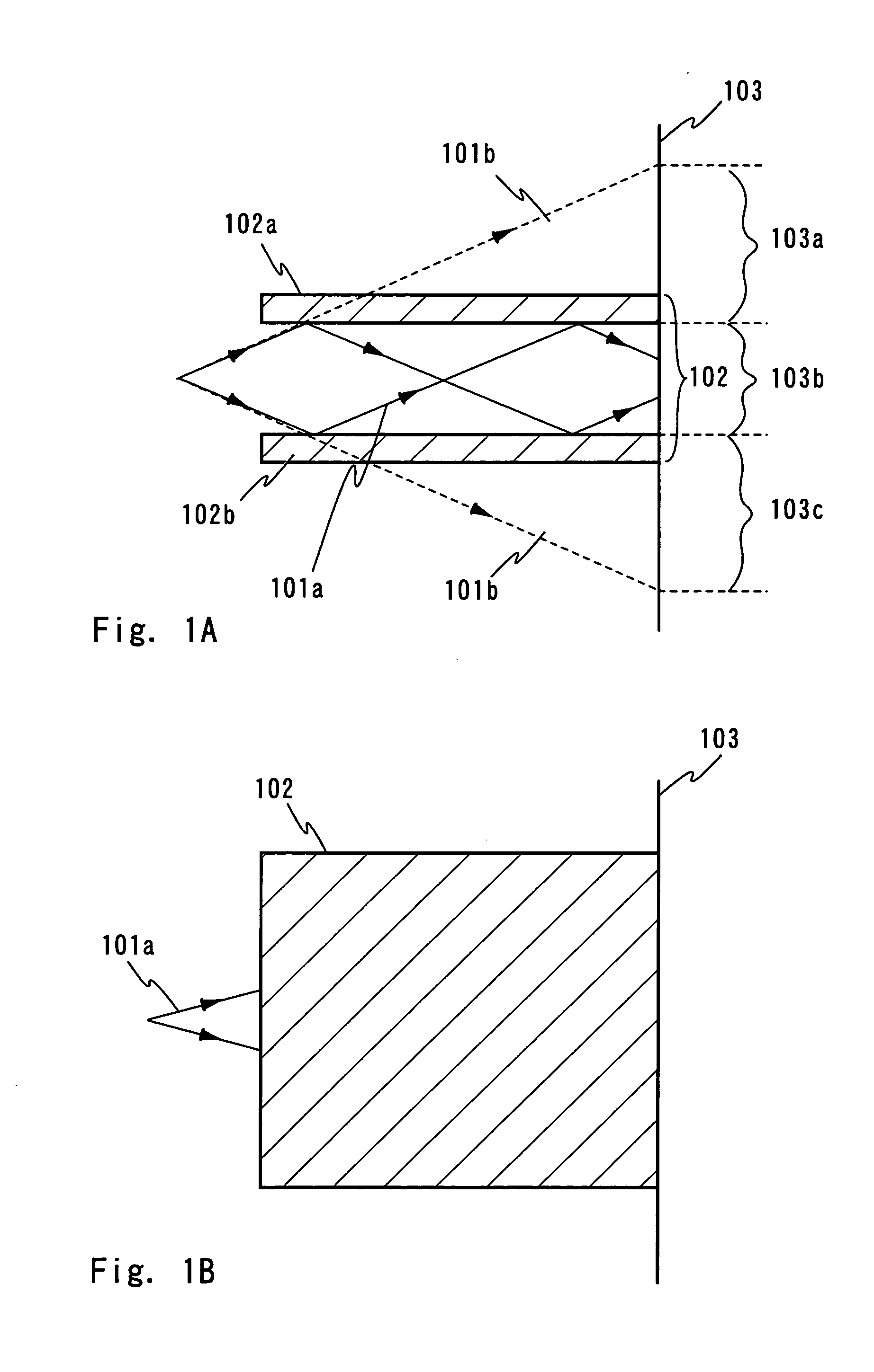
[0087] In FIGS. 5A and 5B, the laser beam goes through the same optical path as that shown in FIGS. 3A and 3B except when the laser beam goes through the optical waveguides 504 and 507. Each of the optical waveguides 504 and 507 has a pair of reflection planes provided oppositely as well as the optical waveguide 304. The optical waveguide 304 has a hollow space between the pair of reflection planes. On the other hand, the optical waveguides 504 and 507 have the space filled with the medium having a refractive index of "n" (>1). This is the different point between these optical waveguides. When the laser ...


PUM


Abstract

The present invention provides a beam homogenizer being able to form a rectangular beam spot having homogeneous energy distribution in a direction of its major axis without using the optical lens requiring to be manufactured with high accuracy. In addition, the present invention provides a laser irradiation apparatus being able to irradiate the laser beam having homogeneous energy distribution in a direction of its major axis. Furthermore, the present invention provides a method for manufacturing a semiconductor device being able to enhance crystallinity in the surface of the substrate and to manufacture TFT with a high operating characteristic. The beam homogenizer, one of the present invention, is to shape the beam spot on the surface to be irradiated into a rectangular spot having an aspect ratio of 10 or more, preferably 100 or more, and comprises an optical waveguide for homogenizing the energy distribution of the rectangular beam spot in the direction of its major axis.

Description

[0001] 1. Field of the Invention[0002] The present invention relates to a beam homogenizer for homogenizing a beam spot on a surface to be irradiated in a certain region. The present invention also relates to a laser irradiation apparatus for irradiating the surface to be irradiated with the beam spot. Furthermore, the present invention also relates to a method for manufacturing a semiconductor device using a crystalline semiconductor film formed with the laser irradiation apparatus.[0003] 2. Description of the Related Art[0004] In recent years, there has been a technique widely studied for crystallizing or enhancing a crystallinity of an amorphous semiconductor film or a crystalline semiconductor film (a semiconductor film having a crystallinity such as poly-crystal or micro-crystal, which is not single-crystal), that is to say, a semiconductor film which is not single-crystal (referred to as a non-single crystalline semiconductor film) formed over an insulating surface such as a g...

Claims


Application Information

Patent Timeline
IPC IPC(8): G02B6/42G02F1/13G02B27/09H01S3/00
CPCG02B6/4204G02B27/0966G02B27/0994H01S3/005G02F1/13
Inventor TANAKA, KOICHIROMORIWAKA, TOMOAKI
Owner SEMICON ENERGY LAB CO LTD
Why Eureka
Try Eureka