Multilayer circuit board and method for manufacturing the same

a multi-layer circuit board and manufacturing method technology, applied in the direction of printing element electric connection formation, transportation and packaging, other domestic articles, etc., can solve the problems of moisture absorption reflow test, insufficient compression cannot be achieved,

Inactive Publication Date: 2004-11-25
PANASONIC CORP
View PDF10 Cites 41 Cited by
  • Summary
  • Abstract
  • Description
  • Claims
  • Application Information

AI Technical Summary

Benefits of technology

[0007] The present invention was arrived at to solve the above issues, and it is an object thereof to provide a multilayer circuit board, and a method for manufacturing the same, wherein the conductive paste is sufficiently compressed during hot pressing to yield a stable electrical connection, and the thermosetting resin can be filled in between the inner layer wiring pattern without leaving gaps.

Problems solved by technology

As a result sufficient compression cannot be attained, and this causes connection defects.
Alternatively, a high degree of curing leads to insufficient adherence with the inner layer substrate and causes whitening due to the resin not sufficiently flowing in between the wiring pattern of the inner layer, and defects result in the moisture absorption reflow test.
If they are made too rigid, however, then they interfere with the ability to bury the resin in the inner layer pattern, and this causes whitening.

Method used


Image

  • Multilayer circuit board and method for manufacturing the same
  • Multilayer circuit board and method for manufacturing the same
  • Multilayer circuit board and method for manufacturing the same

Examples


first embodiment

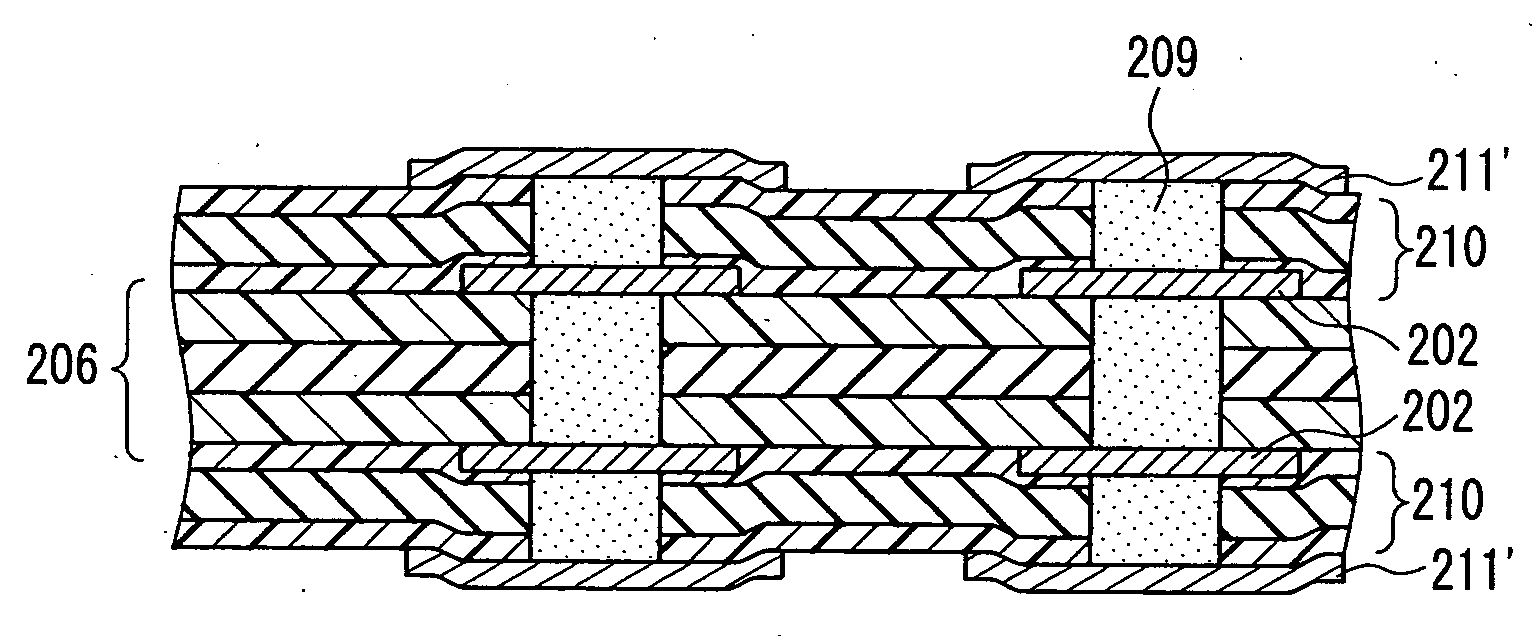
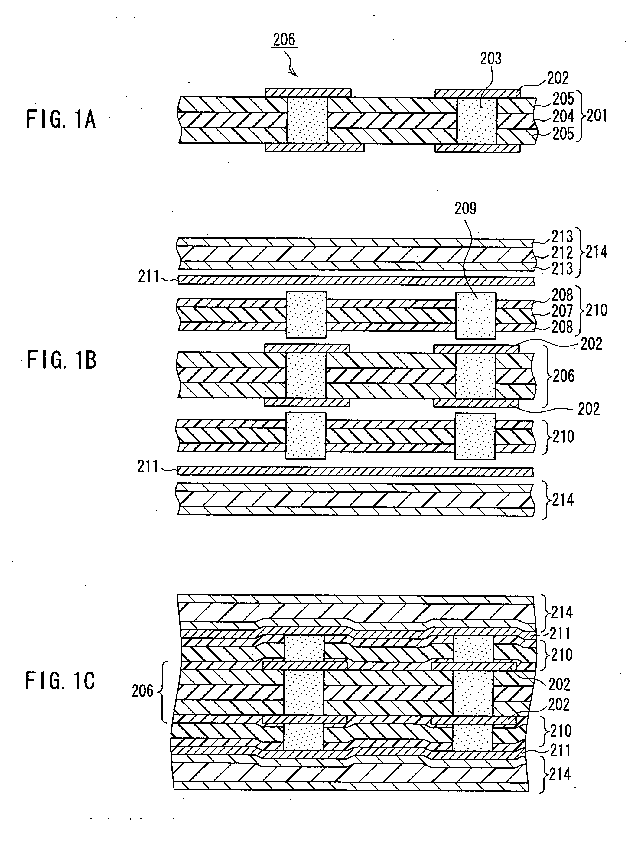
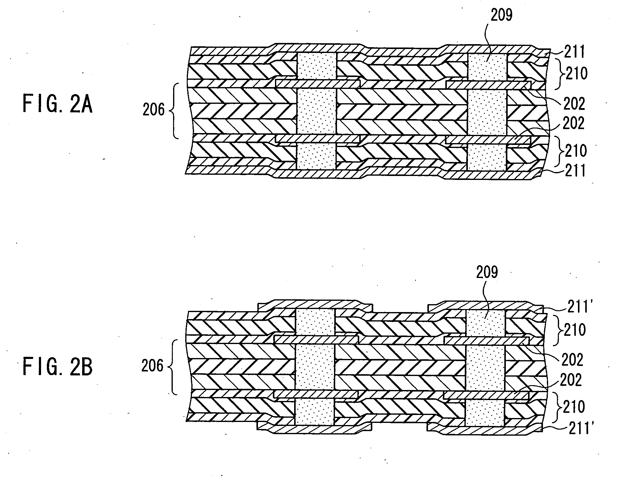
[0029] A method for manufacturing a multilayer circuit board according to the present invention is described with reference to FIGS. 1A to 2B. FIG. 1A shows an inner layer substrate 206 in which wiring layers 202 are formed on both sides of an electrically insulating substrate 201 and these layers are connected by conductive paste 203 or electrolytic plating, for example. The electrically insulating substrate 201 is fabricated by impregnating both sides of a core material 204 with a thermosetting resin 205.

[0030] FIG. 1B shows substrates A 210 disposed on both sides of the inner layer substrate 206. The substrates A 210 are formed by adhering an uncured thermosetting resin 208 to a core material 207 and providing through holes into which a conductive paste 209 is filled. The core material is preferably a heat-resistant synthetic resin film such as a polyimide film, polyamide film, or a fluorine resin film (such as polytetrafluoroethylene) having a thickness in the range of 3 to 50 ....

second embodiment

[0043] The method for manufacturing a multilayer circuit board according to the second embodiment differs from that of the first embodiment discussed above in that it has a step of performing lamination with elastic sheets in a temperature range where the curable uncured resin is not completely cured, rather than using a composite sheet, when hot pressing, and a step of curing the electrically insulating substrate and the conductive paste and establishing electrical connection by hot pressing. The manufacturing method of the second embodiment is described below with reference to FIGS. 3A to 3C. FIG. 3A shows a plurality of substrates, which were fabricated as in FIG. 1B discussed above in the first embodiment, sandwiched between elastic sheets 320. As regards the plurality of substrates, substrates A310, which are obtained by impregnating both sides of a core material 302 with uncured thermosetting resin 303 and providing through holes into which conductive paste 304 is filled are d...

third embodiment

[0047] The method for manufacturing a multilayer circuit board according to the third embodiment differs from that of the first embodiment and the second embodiment discussed above in that it has a step of performing lamination with elastic rolls in a temperature range where a curable uncured resin is not completely cured, rather than using a composite sheet, when hot pressing, and a step of curing the electrically insulating substrate and the conductive paste and establishing electrical connection by hot pressing. The manufacturing method of the third embodiment is described below with reference to FIGS. 4A to 4C. FIG. 4A shows a plurality of substrates fabricated as in FIG. 1B discussed above in the first embodiment sandwiched between elastic rolls 420. Silicone rubber or urethane rubber rolls, for example, can be used as the elastic rolls 420.

[0048] Regarding the plurality of substrates, substrates A410 obtained by impregnating both sides of a core material 402 with uncured therm...


PUM

PropertyMeasurementUnit
heightaaaaaaaaaa
thicknessaaaaaaaaaa
thickaaaaaaaaaa

Abstract

It is an object of the present invention to provide a multilayer circuit board, and a method for manufacturing the same, in which a plurality of circuit boards are layered, wherein as regards at least one circuit board positioned on an outer side, a conductive substance is filled into holes passing through the circuit board in the thickness direction and cured, and the wiring layers of the plurality of circuit boards are electrically connected by the conductive substance that has been cured, wherein in the multilayer circuit board, the wiring layer positioned outside the conductive substance that has been cured projects outward from its surroundings. Thus, the conductive paste is sufficiently compressed during hot pressing to yield a stable electrical connection, and thermosetting resin can be filled in between the inner layer wiring pattern without leaving gaps.

Description

[0001] 1. Field of the Invention[0002] The present invention relates to multilayer circuit boards in which the layers are electrically connected in the thickness direction of the circuit boards with a conductor such as conductive paste, and methods for manufacturing the same.[0003] 2. Description of the Related Art[0004] As electrical devices have become more compact-and more powerful in recent years a great need has developed to inexpensively supply industrial and consumer devices with multilayer wiring circuit boards on which semiconductor chips such as LSIs can be mounted at a high density. In such multilayer wiring circuit boards it is imperative that the plurality of layers of wiring patterns formed at a fine wiring pitch are electrically connected to one another with high reliability. In order to meet these market demands, any layer IVH structure resin multilayer circuit boards employing an inner-via hole connection method that allows interlayer connection of any electrode of ...

Claims


Application Information

Patent Timeline
Patent Type & Authority Applications(United States)
IPC IPC(8): H05K1/11H05K3/40H05K3/46
CPCH05K1/113H05K3/4069H05K3/4614H05K3/4652H05K2201/0195H05K2201/09045Y10T29/49126H05K2201/10378H05K2203/068H05K2203/1461Y10S428/901Y10T29/49124Y10T428/24917H05K2201/096
Inventor NAKATANI, YASUHIROHIGASHITANI, HIDEKINAKAMURA, TADASHIECHIGO, FUMIO
Owner PANASONIC CORP
Why Eureka
Try Eureka