Optical device

Inactive Publication Date: 2004-11-25
IR GVON KHAN
View PDF9 Cites 45 Cited by
  • Summary
  • Abstract
  • Description
  • Claims
  • Application Information

AI Technical Summary

Problems solved by technology

The known dichroic polarizers and retarders have, however, a number of disadvantages--high cost and low thermostability (.about.80.degree. C.
The main disadvantages of said device and LCD on its basis (U.S. Pat. No. 5,751,389) are restricted polarizer size (2.5.times.8 cm.sup.2) and high cost due to technological complexity, therefore it is difficult to realize mass production thereof, because of necessity to use deep vacuum to form oriented film with dyes, and high temperature (up to 300.degree. C.)

Method used


Image

  • Optical device
  • Optical device
  • Optical device

Examples


examples 2-30

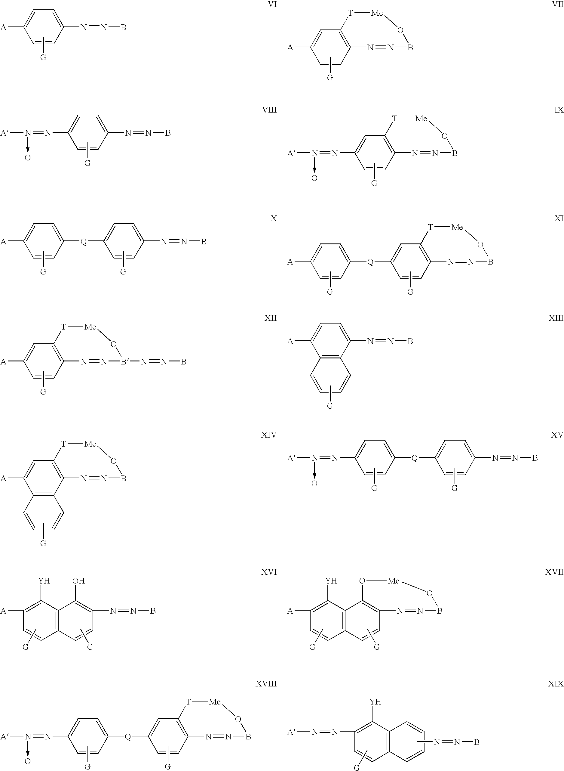
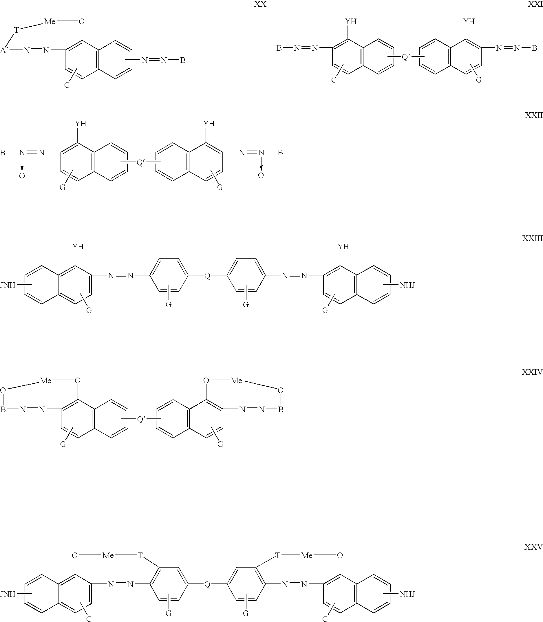
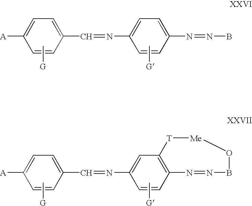
[0133] An optical devices based on other dyes can be prepared in the similar way (see Table in p. 24).

example 31

Fabrication of the Claimed Optical Device as a Homogeneous Phase Delay Layer (Retarder with an Optical Axis Parallel to the Surface)

[0134] LLC composition based on the dye (see Table in p. 24, example 3), transparent in a visible wavelengths range was applied using a rolling cylinder on the surface of a glass plate coated with a transparent conducting layer ITO. After solvent vaporization, molecular oriented layer of 0.9 .mu.m thickness was formed on the plate surface with the optical axis parallel to the surface of the layer. The value of the phase delay (retardation) R was equal 0.27 .mu.m for polarized light falling perpendicularly to the surface of the layer, the highest refractive index was along the optical axis. Anisotropic absorbing fragments of molecules of the dichroic material of said layer were parallel to the optical axis of the layer, and the absorption existed only in UV range (less than 390 nm).

example 32

Fabrication of the Claimed Optical Device as an Inclined Phase Delay Layer (Inclined or Non-Symmetrical Retarder)

[0135] LLC composition containing 9% of dye (see Table in p. 24, example 3) and comprising as one of cations dodecylammonium, providing hydrophoby, was coated using a doctor blade on the surface of a PET film. After drying at a room temperature, 0.3 .mu.m molecular oriented layer was formed with the optic axis parallel to the surface of the layer. The value of phase delay R was equal 0.09 .mu.m (i.e. 90 nm) for a polarized light falling perpendicularly to the surface of the layer, the highest refractive index was parallel to the direction approximately at 40.degree. to the coating direction. Anisotropically absorbing fragments of dichroic material molecules of said layer were directed at angle 40.degree. to the coating direction, and the absorption was present only in UV range (less than 390 nm). The formed layer was then transferred on the surface of a glass plate with t...


PUM

PropertyMeasurementUnit
Thicknessaaaaaaaaaa
Wavelengthaaaaaaaaaa
Thicknessaaaaaaaaaa

Abstract

The invention relates to optical devices for producing and/or transforming polarised electromagnetic emission by means of anisotropic absorption and/or optical rotation effects and/or birefringence and can be used as different polarizers (dichroic, reflecting), lagging layers (retarders), liquid-crystal displays and indicators and also for producing polarising glass for building construction and for sun and antiglare glasses, masks, aprons and faceplates. The inventive optical device is based on at least one molecularly oriented layer of a low-molecular or oligomeric dichroic material which can form a stable lyotropic liquid crystal structure. The projection of at least one anisotropically absorbing fragment of a molecule of the dichroic material on the surface of the molecularly oriented layer of a dipole moment of optical transition is disposed in a parallel position to the optical axis of the molecularly oriented layer at least within several ranges of wavelength of the electromagnetic emission.

Description

[0001] The present invention relates to the field of optics, namely to optical devices for creation and / or transformation of polarized electromagnetic radiation due to effects of anisotropic absorption and / or optical rotation and / or birefringence effect.[0002] The present optical device can be used as polarizers of various types (dichroic, reflective), phase delay layers or coatings (retarders), liquid crystal displays (LCD) and indicators, information display devices, in production of optical instruments, in manufacturing of polarization glass for building construction, in lighting equipment, and also for fabrication of sun-protection and antiglare glasses, masks, shields, visors, polarization pictures, advertising, security facilities of trademarks or securities.DESCRIPTION OF THE RELATED ART[0003] At the present time for conversion of unpolarized electromagnetic radiation (for example visible light) into polarized one optical devices are widely used consisting of dichroic polariz...

Claims


Application Information

Patent Timeline
IPC IPC(8): C09B23/00C09B35/029C09B35/16C09B35/52C09B45/26C09B45/28C09B45/30C09B45/32C09B56/00C09B56/06C09B57/00G02B5/30G02F1/13G02F1/1334G02F1/1335G02F1/13363
CPCG02B5/3016Y10T428/1036Y10T428/1005Y10T428/10C09K2323/00C09K2323/02C09K2323/03G02B5/30
Inventor KHAN, IR GVONBELYAEV, SERGEJ VASILIEVICHVOROZHTSOV, GREGORY NIKOLAEVICHKUKUSHKINA, MARIA LEONARDOVNAMALIMONENKO, NIKOLAI VALDIMIROVICHMASANOVA, NATALIYA NIKOLAEVNAMOSCOW, ELENA YURIEVNATAMBIEVA, OLGA AKHMATOVNA
Owner IR GVON KHAN
Why Eureka
Try Eureka