

Adhesive tape
a technology of adhesive tape and adhesive layer, applied in the direction of heat-activated film/foil adhesive, semiconductor/solid-state device details, instruments, etc., can solve the problems of inability to achieve satisfactory bonding strength, difficulty in applying an appropriate amount of adhesive, and overflowing of adhesive ic chips, etc., to prevent package cracking, excellent ability, and reduce the elastic modulus at thermocompression bonding
Inactive Publication Date: 2004-11-25
LINTEC CORP
View PDF4 Cites 37 Cited by
- Summary
- Abstract
- Description
- Claims
- Application Information
AI Technical Summary
Benefits of technology
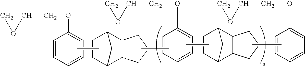
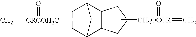
The present invention provides an adhesive tape with an adhesive layer that reduces water absorption and lowers the elastic modulus at thermocompression bonding. This is achieved by using an adhesive layer that includes an adherent component, an epoxy resin, a thermally active latent epoxy resin curing agent, an energy radiation polymerizable compound, and a photopolymerization initiator. The epoxy resin has a dicyclopentadiene skeleton and the energy radiation polymerizable compound has a dicyclopentadiene skeleton. The adhesive tape has high capability of following the contour of the adherend surface and is suitable for use in various applications.
Problems solved by technology
However, when IC chips are extremely small, application of an appropriate amount of adhesive is difficult, and there has occurred such a problem that the adhesive overflows IC chips.
On the other hand, when IC chips are large, there has occurred such a problem that the bonding with satisfactory strength cannot be attained because of, for example, an insufficient amount of adhesive.
Further, the application of such a die bonding adhesive is laborious.
The melting temperature of the solders not containing lead is higher than that of conventional solder containing lead, thereby rendering high reflow temperatures inevitable.
However, when the reflow temperature is high, even a small amount of water contained in the adhesive layer would vaporize and inflate, thereby causing the danger of package cracking.
However, the above conventional adhesives are unsatisfactory in this respect.
Method used
View moreImage
Smart ImageViewing Examples


Examples
example 1
[0103] An adhesive composition was obtained by mixing the components together in the proportions as specified in Table 1. A base of a 90 .mu.m thick laminate film composed of a plasticized PVC layer and a layer of ethylene / methacrylic acid copolymer on its side of ethylene / methacrylic acid copolymer layer (surface tension: 35 dyn / cm) was coated with this adhesive composition so that a 20 .mu.m adhesive layer was formed on the base. Thus, an adhesive tape was obtained.
[0104] The "water absorption coefficient", "elastic modulus" and "peel strength" of the obtained adhesive tape were measured in the above manners. The results are listed in Table 1.
Login to View More PUM
| Property | Measurement | Unit |
|---|---|---|
| temperature | aaaaa | aaaaa |
| temperature | aaaaa | aaaaa |
| glass transition temperature | aaaaa | aaaaa |
Abstract
An adhesive tape comprising a base and, superimposed thereon, an adhesive layer, this adhesive layer comprising an adherent component (A), an epoxy resin (B), a thermally active latent epoxy resin curing agent (C), an energy radiation polymerizable compound (D) and a photopolymerization initiator (E), wherein either or both of the epoxy resin (B) and energy radiation polymerizable compound (D) have a dicyclopentadiene skeleton in its molecule or molecules thereof. The resultant adhesive tape has an adhesive layer which provides reduced water absorption of an adhesive curing product and which enables a lowering of the elastic modulus thereof during thermocompression bonding.
Description
[0001] The present invention relates to a novel pressure sensitive adhesive tape. More particularly, the present invention relates to a pressure sensitive adhesive tape which is especially suitable for use in the process of dicing a silicon wafer or the like and performing die bonding of chips obtained by the dicing to a lead frame.[0002] A semiconductor wafer of, for example, silicon or gallium arsenide is produced in the form of a large diameter. This wafer is cut and separated (diced) into small element chips (IC chips) and is transferred to the subsequent mounting step. In this process, in particular, the semiconductor wafer in the state of being stuck to a pressure sensitive adhesive tape is subjected to dicing, cleaning, drying, expanding and pickup steps, and is transferred to the subsequent bonding step.[0003] It is desired that the above pressure sensitive adhesive tape employed from the semiconductor wafer dicing step through the pickup step have an adhesive strength which...
Claims
Login to View More Application Information
Patent Timeline
 Patent Type & AuthorityApplications(United States)
IPC IPC(8): C08G59/24C08G59/32C08G59/40C08K5/00C08K5/103C09J4/00C09J7/22C09J7/35C09J7/38C09J163/00G03F7/038H01L21/52H01L21/68
CPCC08G59/24Y10T428/2891C08G59/4021C08K5/0025C08K5/103C09J7/0203C09J7/0242C09J7/0246C09J163/00C09J2203/326C09J2463/00G03F7/038H01L21/6836H01L2221/68327C08G59/3218Y10T428/2852Y10T428/287H01L2924/0002C08L2666/04C08L2666/02H01L2924/00C09J7/35C09J7/38C09J7/22Y10T428/31511
InventorSUMI, TAKAJIYAMAZAKI, OSAMUSUGINO, TAKASHISENOO, HIDEO
OwnerLINTEC CORP