Method for treating semiconductor processing components and components formed thereby

a technology for semiconductor processing components and components, applied in the direction of silicon carbide, transportation and packaging, carbide, etc., can solve the problems of insufficiently addressing certain contamination issues, and the technology appears limited to restoring pre-machined purity levels to the componen

Inactive Publication Date: 2004-11-25
SAINT GOBAIN CERAMICS & PLASTICS INC
View PDF66 Cites 9 Cited by
  • Summary
  • Abstract
  • Description
  • Claims
  • Application Information

AI Technical Summary

Problems solved by technology

The desire for superior purity levels and larger wafers introduces further integration challenges for next generation processing.
However, the techniques disclosed therein do not adequately address certain contamination issues, and appear to

Method used


Image

  • Method for treating semiconductor processing components and components formed thereby
  • Method for treating semiconductor processing components and components formed thereby
  • Method for treating semiconductor processing components and components formed thereby

Examples


Embodiment Construction

)

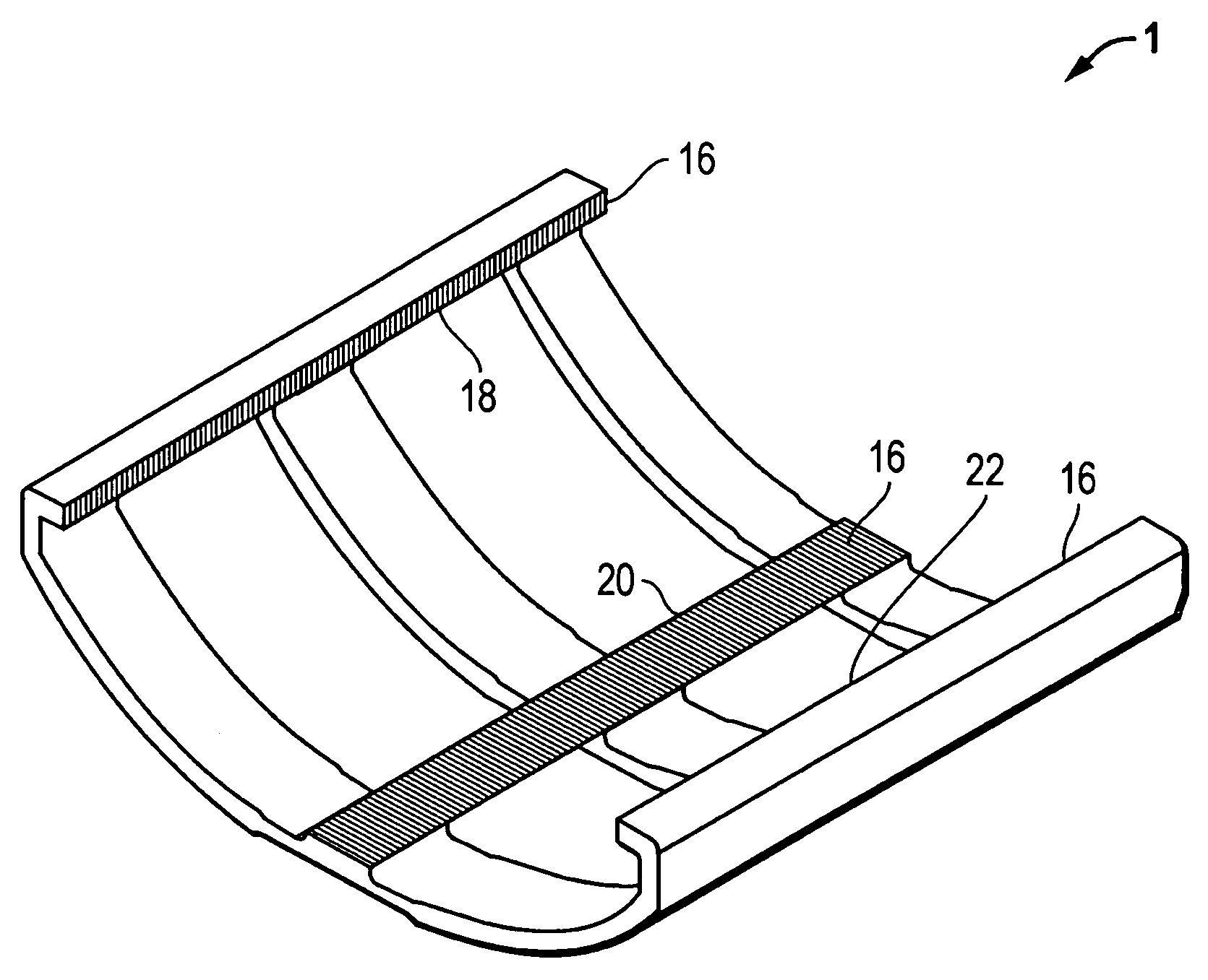
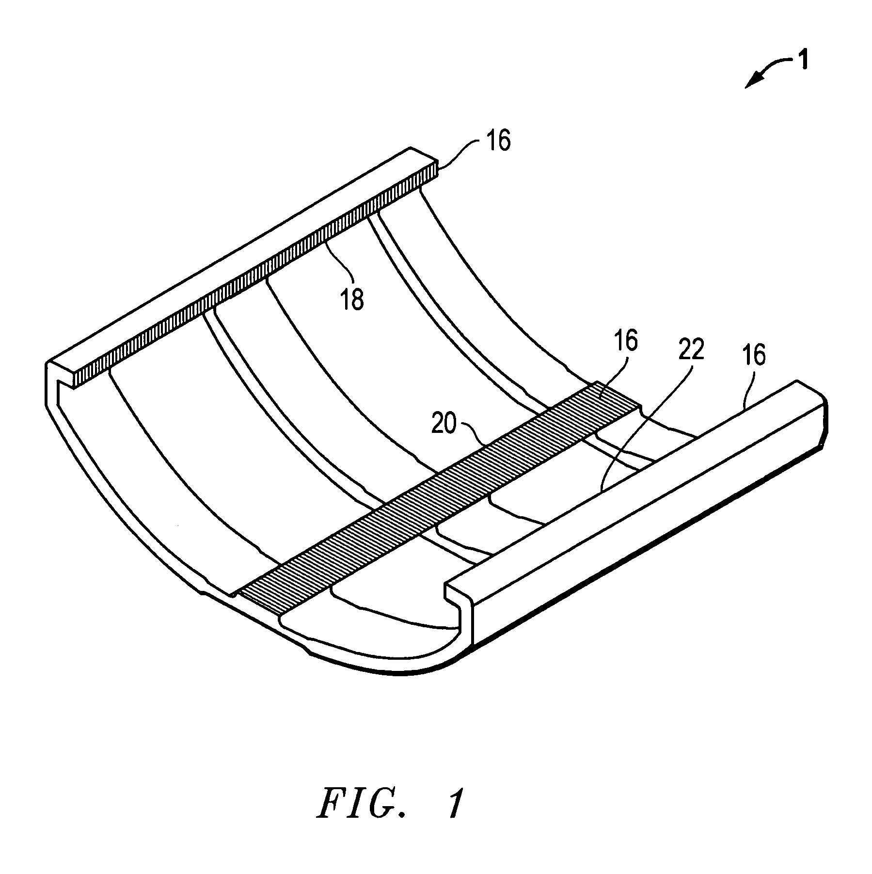
[0018] According to aspects of the present invention, a semiconductor processing component, and a method for treating a semiconductor processing component are provided. The semiconductor processing component generally is formed at least partially of SiC, including an outer surface portion that has a controlled impurity content. The outer surface portion is typically formed by chemical vapor deposition (CVD), and has an outer purity that is not greater than ten times a bulk purity. The outer surface portion may be defined as an identifiable SiC layer formed by CVD, or an outer thickness of a SiC component formed principally by CVD, as in the case of free-standing CVD-SiC components, described in more detail below.

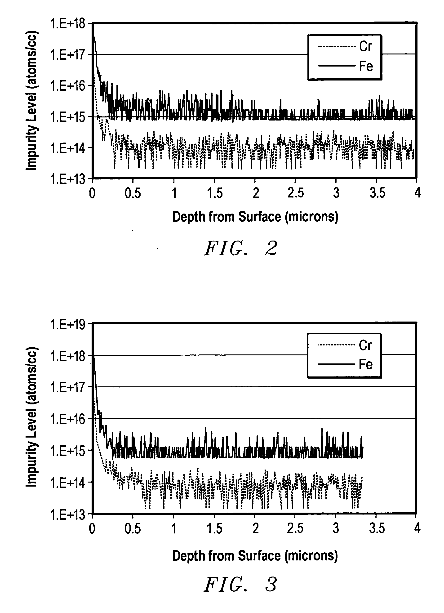
[0019] According to one aspect, the present inventors have recognized that as-deposited CVD-SiC has a spike in impurity levels at the outer surface thereof, typically within the first 0.5 .mu.m, such as within the first 0.25 .mu.m, or the first 0.10 .mu.m of the outer depth...


PUM

PropertyMeasurementUnit
Fractionaaaaaaaaaa
Temperatureaaaaaaaaaa
Thicknessaaaaaaaaaa

Abstract

A semiconductor processing component formed of SiC, wherein an outer surface portion of the component has a surface impurity level that is not greater than ten times a bulk impurity level of the outer surface portion.

Description

CROSS-REFERENCE TO RELATED APPLICATION(S)[0001] This application is a continuation-in-part application of U.S. 10 / 414,563, filed Apr. 15, 2003, and claims priority thereto under 35 USC 120.[0002] 1. Field of the Invention[0003] The present invention is generally related to methods for treating semiconductor processing components for use in a semiconductor fabrication environment, as well as semiconductor processing components formed thereby.[0004] 2. Description of the Related Art[0005] In the art of semiconductor processing, typically integrated circuit devices are formed through various wafer processing techniques, in which semiconductor (principally silicon) wafers are processed through various stations or tools. Processing operations include, for example, high temperature diffusion, thermal processing, ion implant, annealing, photolithography, polishing, deposition, etc. As new generation semiconductor devices are developed, an intense demand continues to exist in the industry t...

Claims


Application Information

Patent Timeline
IPC IPC(8): C01B31/36C04B35/565C04B35/622C04B41/45C04B41/80H01L21/673
CPCC01B31/36Y10T428/26C04B35/565C04B35/62222C04B41/009C04B41/459C04B41/80C04B2235/3826C04B2235/428C04B2235/72C04B2235/80C04B2235/963H01L21/6733C01P2006/80Y10T428/12576C04B41/4519C04B41/4556C04B41/5035C01B32/956H01L21/322
Inventor NARENDAR, YESHWANTHBUCKLEY, RICHARD F.
Owner SAINT GOBAIN CERAMICS & PLASTICS INC
Why Eureka
Try Eureka