

Hdp-cvd multistep gapfill process
a multi-step, gapfilling technology, applied in the direction of solid-state diffusion coating, chemical vapor deposition coating, diaphragms, etc., can solve the problems of increasing the danger of underlying structure damage, little material is deposited on the sidewalls, and little protection for the structure during the etching phase, so as to reduce the sputtering characteristics and the average molecular weigh
- Summary
- Abstract
- Description
- Claims
- Application Information
AI Technical Summary
Benefits of technology
Problems solved by technology
Method used
Image

Examples
Embodiment Construction
Background of Invention
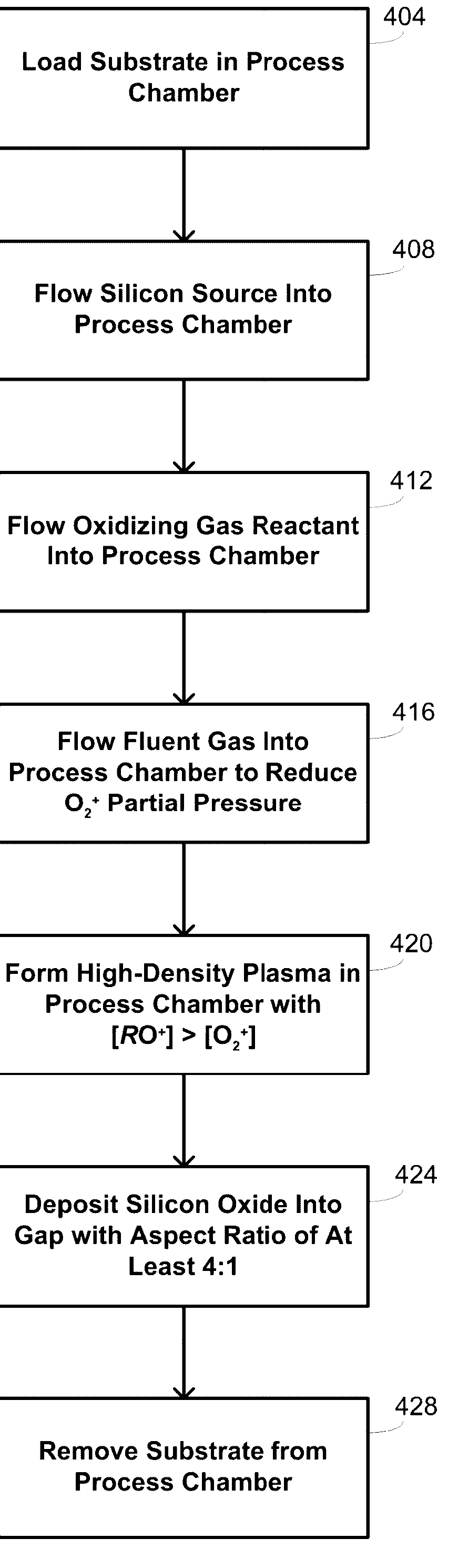
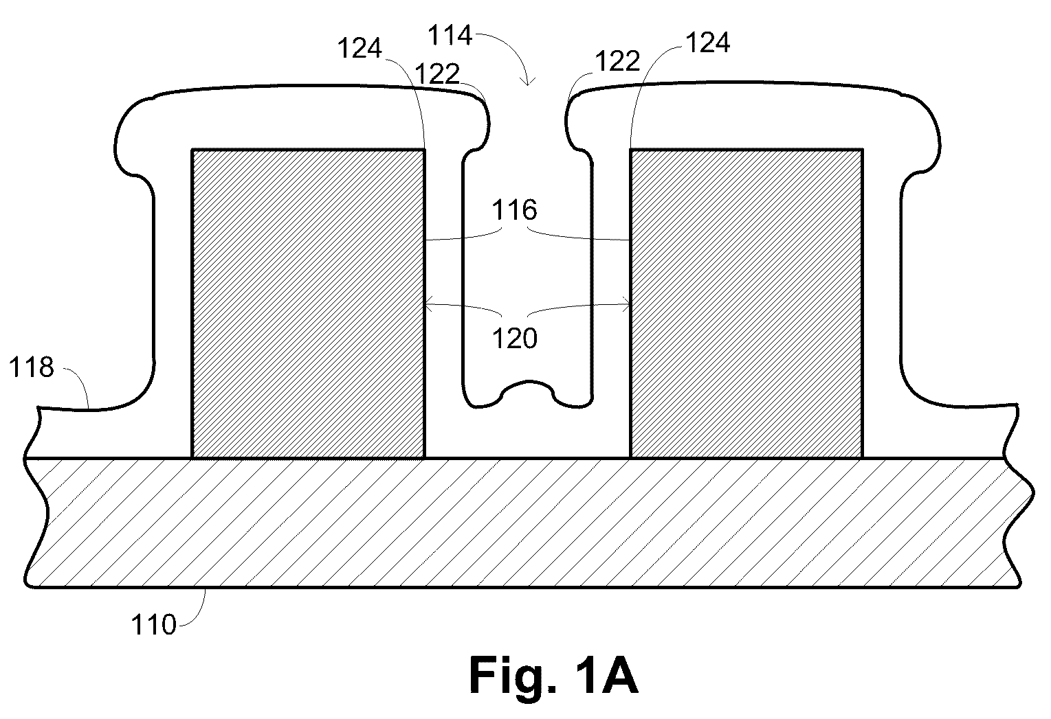
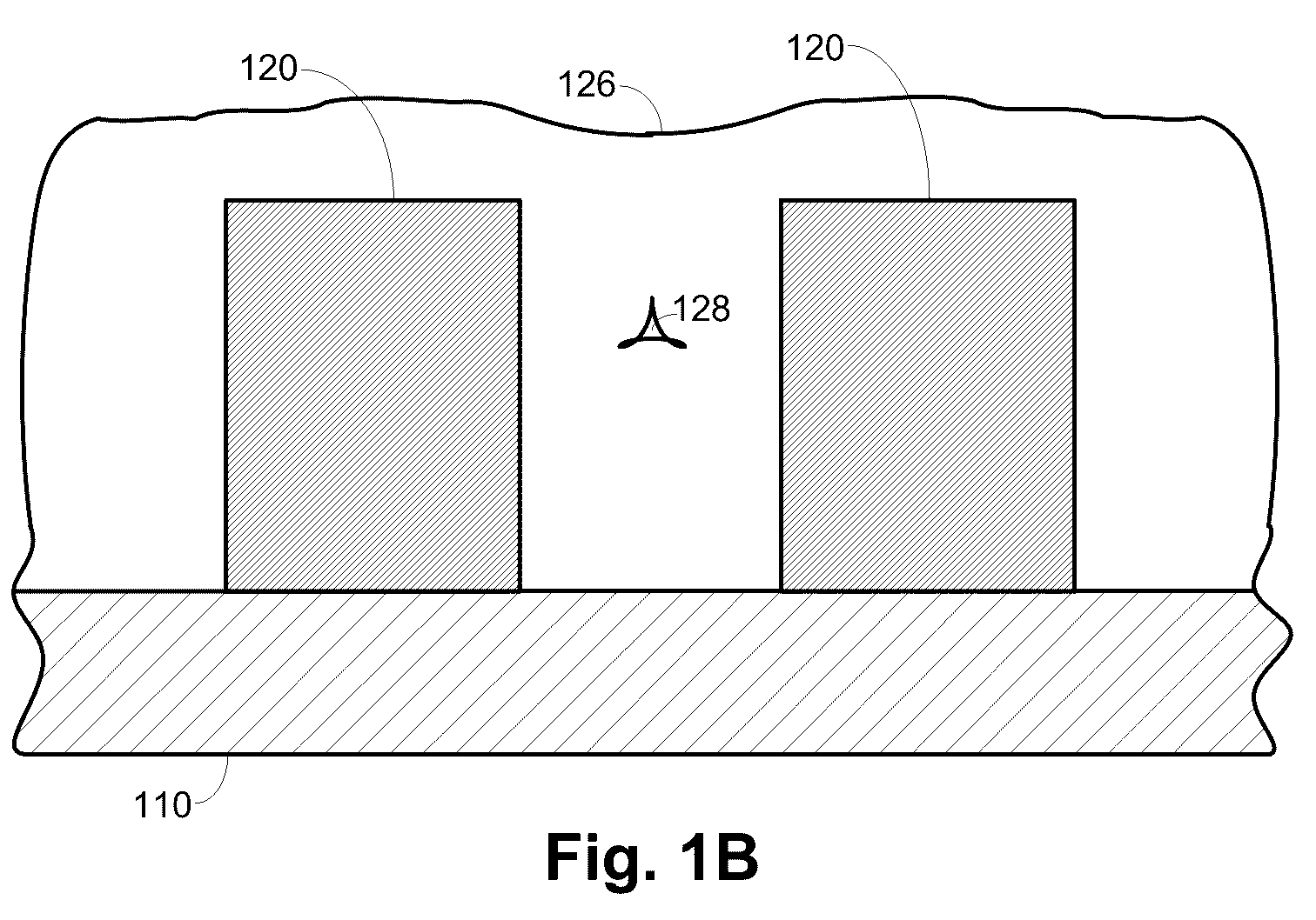
[0001] One of the persistent challenges faced in the development of semiconductor technology is the desire to increase the density of circuit elements and interconnections on substrates without introducing spurious interactions between them. Unwanted interactions are typically prevented by providing gaps or trenches that are filled with electrically insulative material to isolate the elements both physically and electrically. As circuit densities increase, however, the widths of these gaps decrease, increase their aspect ratios and making it progressively more difficult to fill the gaps without leaving voids. The formation of voids when the gap is not filled completely is undesirable because they may adversely affect operation of the completed device, such as by trapping impurities within the insulative material.
[0002] Common techniques that are used in such gapfill applications are chemical-vapor deposition ("CVD") techniques. Conventional thermal CVD process...
PUM
| Property | Measurement | Unit |
|---|---|---|
| temperature | aaaaa | aaaaa |
| ASPECT RATIO | aaaaa | aaaaa |
| temperature | aaaaa | aaaaa |
Abstract
Description
Claims
Application Information