Structure manufacturing method

Inactive Publication Date: 2004-12-16
CANON KK
View PDF15 Cites 41 Cited by
  • Summary
  • Abstract
  • Description
  • Claims
  • Application Information

AI Technical Summary

Problems solved by technology

However, recesses/projections formed on the surface of a metal thin film by agglomerations of grains have a height of several to tens of several nanometers, they can be obstacles when for

Method used


Image

  • Structure manufacturing method
  • Structure manufacturing method
  • Structure manufacturing method

Examples


first embodiment

[0057] In this example, the invention is used.

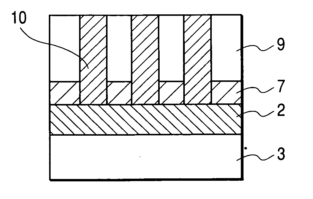
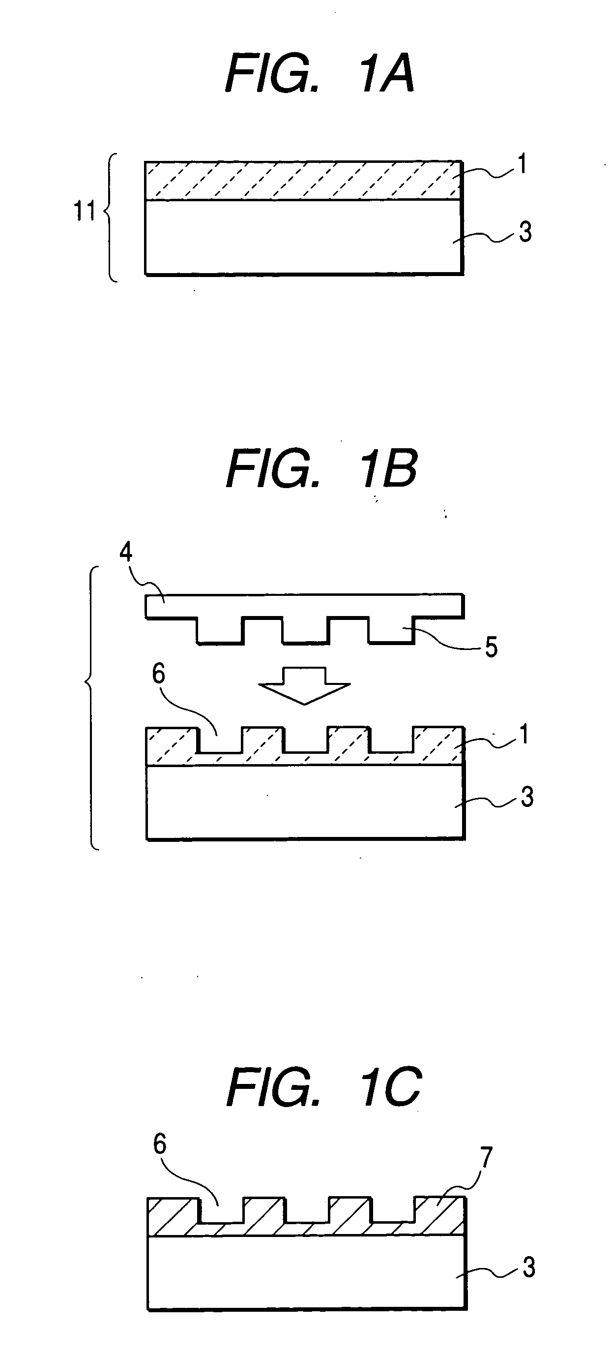
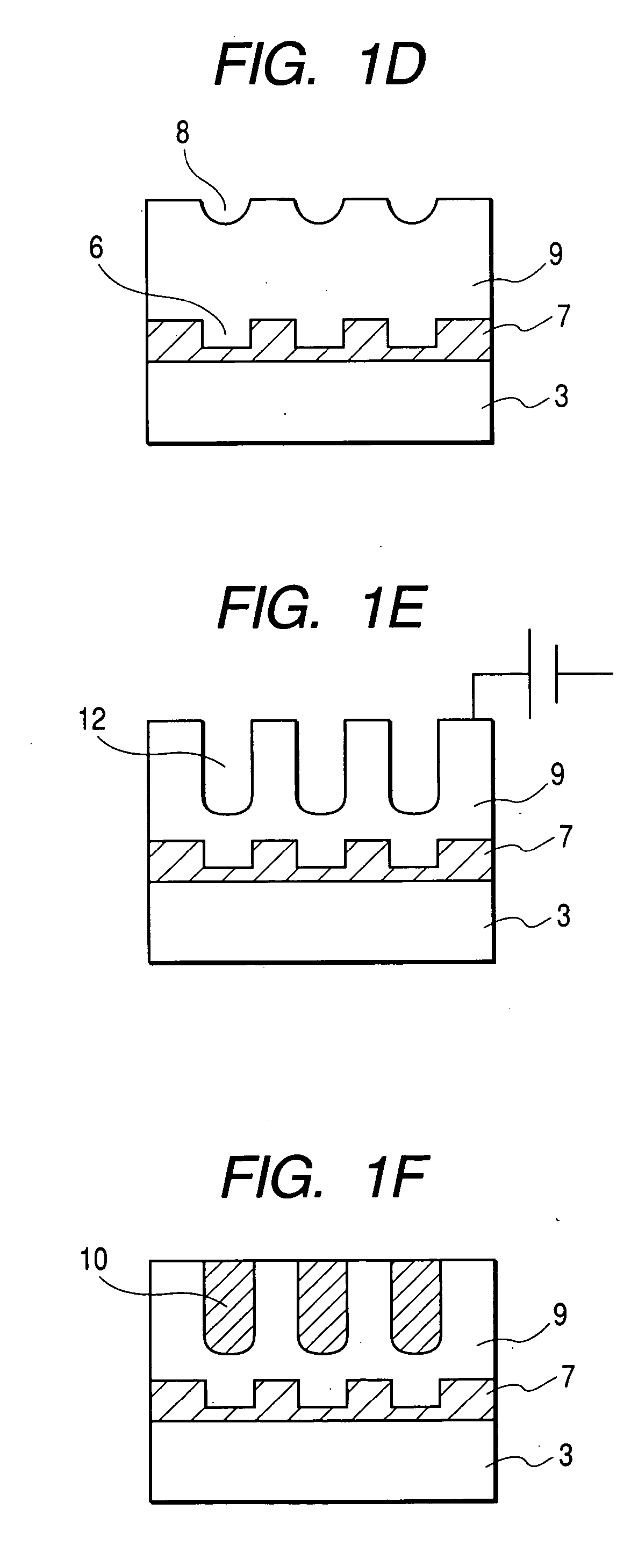
[0058] As shown in FIGS. 1A, 1B, 1C, 1D, 1E and 1F, with the first embodiment of nano-structure manufacturing method, firstly a liquid application material 1 that contains silicon is applied onto a support substrate 3 to produce an object of processing 11 (step (1)). Then, a mold 4 having projection structures 5 with intervals of nanometers is pressed against the layer of the liquid material 1 that contains silicon to produce corresponding recess structures 6 (step (2)). Thereafter, the liquid material is baked in oxygen-containing gas or oxidized in ozone or oxygen plasma to make it electrically highly resistive (step (3)). Subsequently, a layer to be anodized 9 is formed on said oxidized liquid material (step (4)). Then, the layer to be anodized is actually anodized in an acidic solution (step (5)). Finally, fine holes that are aligned with the respective recess structures 6 are formed in the anodized layer 9.

[0059] For instance, as sh...

example 2

[0063] In this example, the second embodiment of the invention is used.

[0064] As shown in FIGS. 2A, 2B, 2C, 2D, 2E, 2F and 2G, with the second embodiment of nano-structure manufacturing method, firstly a liquid application material 1 that contains silicon is thinly applied onto an electro-conductive layer 2 (step (1)). Then, a mold 4 having projection structures 5 with intervals of nanometers is pressed against the layer of the applied liquid material 1 to produce corresponding recess structures 6 on the surface of the silicon-containing liquid material (step (2)). Thereafter, the silicon-containing liquid material is oxidized typically by means of baking so as to make it inorganic and come into an electrically highly resistive state 7 (step (3)). Then, the residue in the recess structures 6 of the silicon-containing liquid material is removed by etching to expose the electro-conductive layer 2 (step (6)). Then, a layer to be anodized 9 is formed on said oxidized insulator (step (4)...

example 3

[0069] In this example, the third embodiment of the invention is used.

[0070] As shown in FIGS. 3A, 3B, 3C, 3D, 3E, 3F and 3G, with the third embodiment of nano-structure manufacturing method, firstly a liquid application material 1 that contains silicon is applied onto an electro-conductive layer 2 (step (1)). Then, a mold 4 having projection structures 5 with intervals of nanometers is pressed against the layer of the applied liquid material 1 to produce corresponding recess structures 6 on the surface of the silicon-containing liquid material 1 (step (2)). Then, the electro-conductive layer 2 is exposed in the areas of the recess structures by etching (step (6')). Thereafter, the silicon-containing liquid material is oxidized by oxidation, which is typically baking (step (3'). Then, a layer 9 to be anodized is formed thereon (step (4)) and then actually anodized (step (7)) to produce nano-structures.

[0071] FIGS. 3A, 3B, 3C, 3D, 3E, 3F and 3G illustrate typical steps of the third e...


PUM

PropertyMeasurementUnit
Electrical conductoraaaaaaaaaa

Abstract

A liquid application material that is capable of forming an oxidized insulator as a result of baking is applied onto a support substrate to produce an object of processing. Then, a mold having projection structures with intervals of nanometers is pressed against the applied liquid material to produce corresponding recess structures. Thereafter, the applied liquid material is baked in oxygen-containing gas or oxidized in ozone or oxygen plasma to make it electrically highly resistive. Subsequently, a layer to be anodized is formed on said oxidized insulator. Then, the layer to be anodized is actually anodized in an acidic solution to form fine holes that are aligned with the respective recess structures in the anodized layer. Accordingly, fine recess structures can be manufactured with ease.

Description

[0001] 1. Field of the Invention[0002] This invention relates to a method of manufacturing recess / projection structures with very fine intervals of a scale of nanometers. This invention also relates to a magnetic device using a structure.[0003] 2. Related Background Art[0004] So-called nano-imprinting methods have been proposed in recent years as techniques for forming micro-structures of dimensions of nanometers on the surface of an object to be processed by directly pressing a mold of recess / projection structures against the object (see, inter alia, U.S. Pat. No. 5,772,905 and Japanese Patent Application Laid-Open No. 2000-232095). They represent new technological developments and do not relate to lithography that uses light and / or an electron beam.[0005] With any of the proposed techniques, a mold 101 prepared through a process using an electron beam as shown in FIGS. 6A, 6B, 6C, 6D and 6E of the accompanying drawings and having a pattern of projection structures that are arrange...

Claims


Application Information

Patent Timeline
IPC IPC(8): B81C1/00B82B3/00B82Y40/00C23C28/00C23C30/00C23F4/00C25D11/04H01L21/44H01L31/072
CPCB81C1/00619Y10T29/49996Y10T29/49924Y10T29/49995
Inventor IMADA, AYADEN, TOHRU
Owner CANON KK
Why Eureka
Try Eureka