Module with a built-in semiconductor and method for producing the same

a technology of built-in semiconductors and modules, which is applied in the association of printed circuit non-printed electric components, dielectric characteristics, radiation controlled devices, etc., can solve the problems of inferior connection between wiring layers, passive components cannot be disposed on the overrunning portion of sealing resin, and the inner via cannot be disposed at a place, etc., to achieve the effect of convenient filling with conductive resin

Inactive Publication Date: 2005-01-06
PANASONIC CORP
View PDF1 Cites 137 Cited by
  • Summary
  • Abstract
  • Description
  • Claims
  • Application Information

AI Technical Summary

Benefits of technology

[0006] The module with a built-in semiconductor of the above construction is produced by a method which includes mounting a semiconductor device on a wiring layer formed on a circuit board, stacking on the circuit board an electrically insulating substrate having inner vias, and heating and pressurizing so that the semiconductor device is buried in the electrically insulating substrate. This production method has an advantage that filling through holes for the inner vias can be easily filled with a conductive resin and that a process for forming the inner via can be selected from a wide range. However, when using this production method, the inner via cannot be disposed at a place where the sealing resin extends over the edge portion of the semiconductor device. This is because when the electrically insulating substrate is stacked, the inner via cannot pierce a portion of the sealing resin which overruns the semiconductor, without deformation. The deformation of the inner via causes inferior connection between the wiring layers. Further, a passive component cannot be disposed on the overrunning portion of the sealing resin. As described above, the overrunning sealing resin reduces an area where the inner vias and the passive components can be mounted. As a result, when it is necessary to dispose a predetermined number of inner vias and passive components each of which has a predetermined size, an area of the module with a built-in semiconductor should be large, which is adverse to the requirement of miniaturization of the electronic equipments.

Problems solved by technology

However, when using this production method, the inner via cannot be disposed at a place where the sealing resin extends over the edge portion of the semiconductor device.
The deformation of the inner via causes inferior connection between the wiring layers.
Further, a passive component cannot be disposed on the overrunning portion of the sealing resin.
As a result, when it is necessary to dispose a predetermined number of inner vias and passive components each of which has a predetermined size, an area of the module with a built-in semiconductor should be large, which is adverse to the requirement of miniaturization of the electronic equipments.
However, when the semiconductor device is incorporated, the device is fixed securely by being surrounded entirely by the electrically insulating core layer in the final module, and therefore there is no practical problem even if the sealing resin is not used.
Therefore, when the functional element-formed surface is covered with the sealing resin as shown in FIG. 18, a high-frequency signal is disadvantageously transmitted, and there may raise a problem of corrosion.

Method used


Image

  • Module with a built-in semiconductor and method for producing the same
  • Module with a built-in semiconductor and method for producing the same
  • Module with a built-in semiconductor and method for producing the same

Examples


example 1

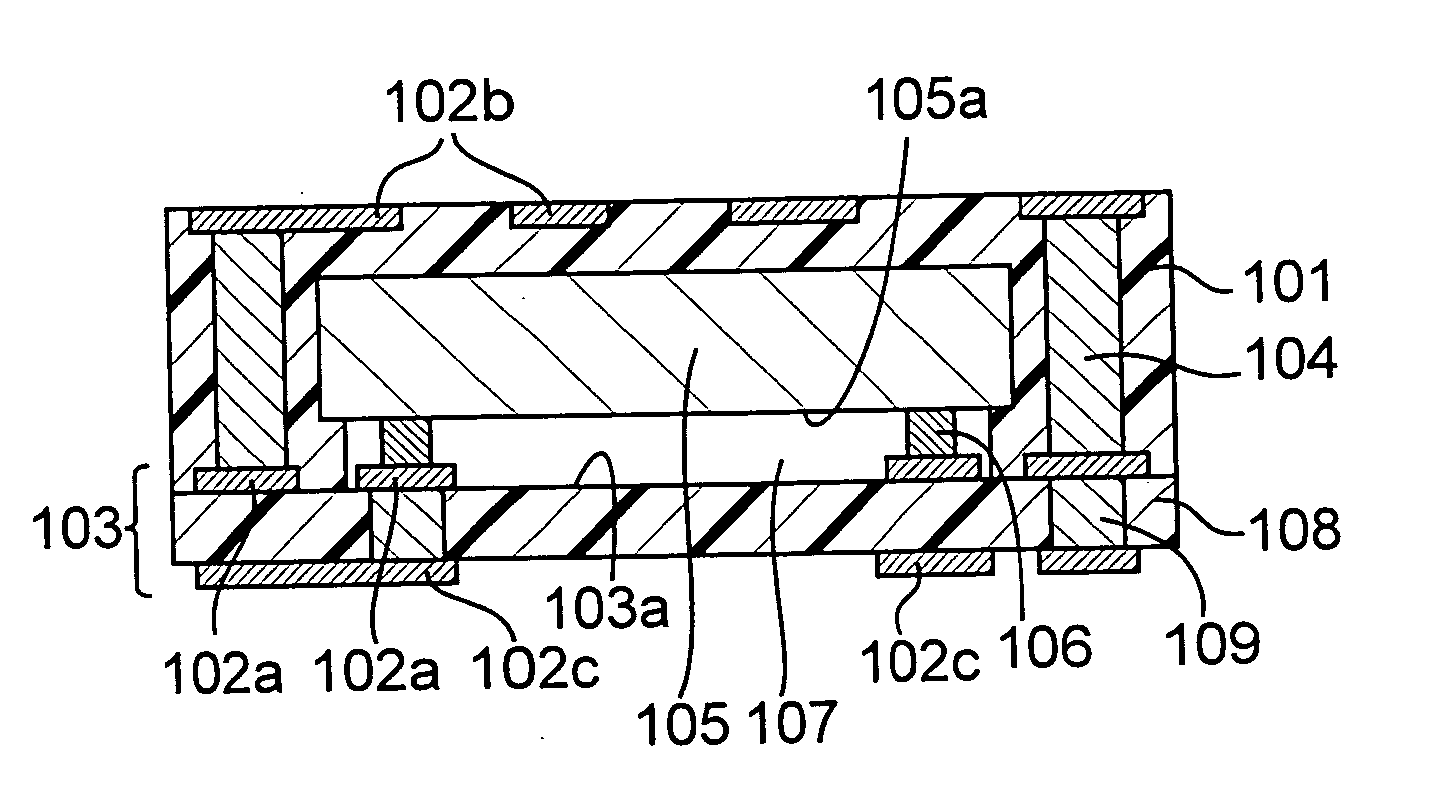
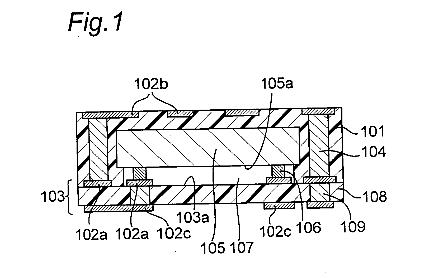
[0164] In Example 1, a module with a built-in semiconductor according to Embodiment 1 was produced according to the following procedures (i) to (iii)

[0165] (i) Manufacturing of Electrically Insulating Substrate

[0166] An electrically insulating substrate was prepared by forming a sheet member from a mixture of an inorganic filler and a thermosetting resin and then forming through bores and filling the bores with a conductive paste. The materials for the sheet member was prepared by charging the inorganic filler, the thermosetting resin and optionally a solvent for adjusting a viscosity into a container having a predetermined volume, and then rotating the container itself and revolving it by means of an agitator. This mixing (or agitation) method makes the inorganic filler dispersed sufficiently (that is, gives a uniform dispersion), even if the mixture has a relative high viscosity. In this example, a mixture of 10 wt % an epoxy resin as the thermosetting resin (including a curing ...
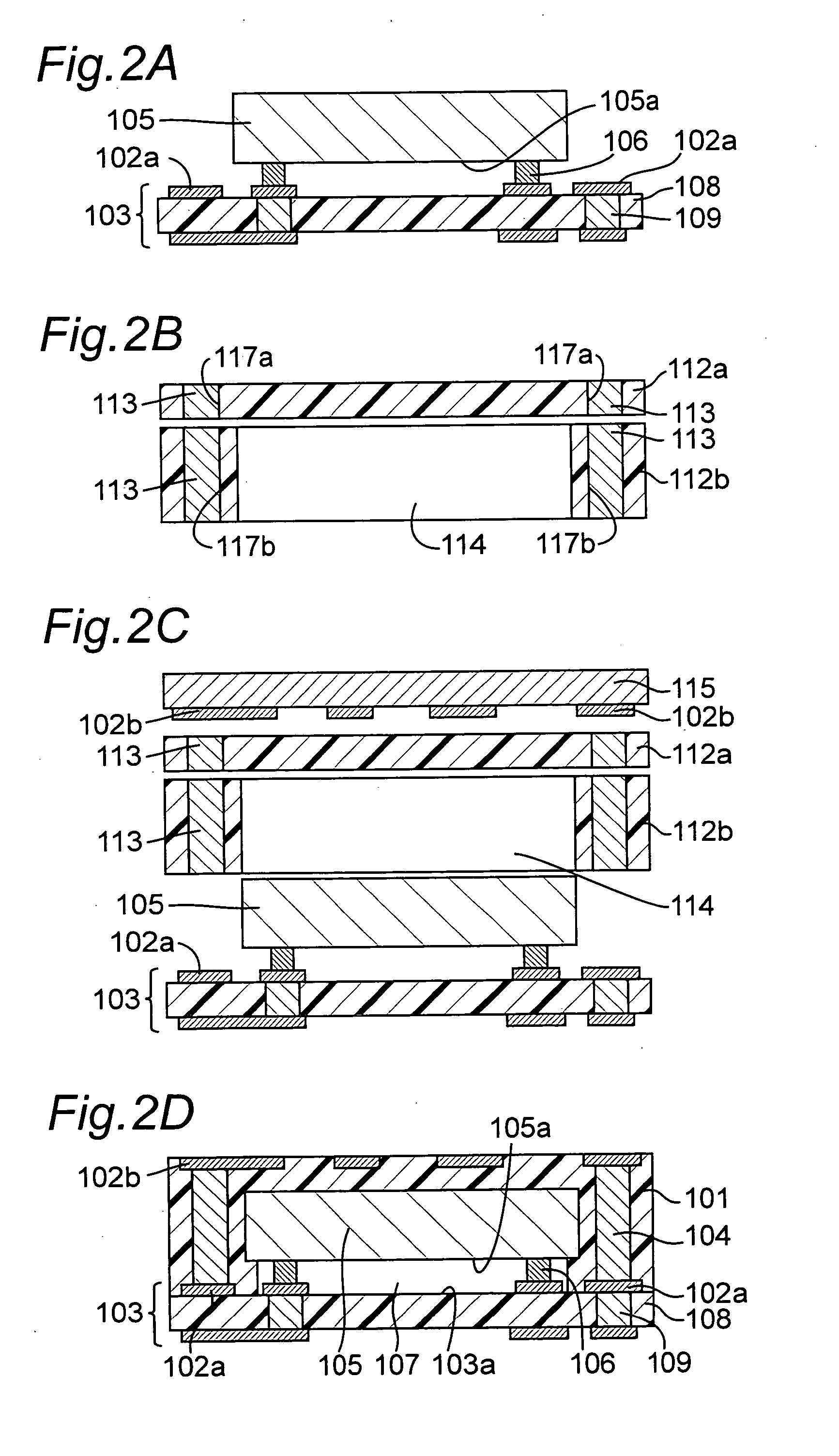
example 2

[0180] In Example 2, a module with a built-in semiconductor of Embodiment 3 was produced. In Example 2, a module was produced by manufacturing, in the same manner as in Example 1, a laminate which consisted of a circuit board with a mounted semiconductor device, two electrically insulating substrates and a mold release film having a wiring layer, and heating and pressurizing the laminate at 120° C. and 1 MPa for 5 minutes and then at 180° C. and 1 MPa for one hour. 120° C. is a temperature in a range of TL+20° C. wherein TL is a temperature at which a thermosetting resin contained in the electrically insulating substrate indicates the lowest melt viscosity. During heating at 120° C., the viscosity of the thermosetting resin which was contained in the electrically insulating substrate declined and the resin was fluidized. Therefore, during the lower temperature heating, the material of the electrically insulating substrate flowed, and surrounded and sealed the protruding electrodes. ...


PUM


Abstract

In a module with a built-in semiconductor, higher densification is achieved by disposing inner vias close to a semiconductor device. A module which has a space 107 between a first wiring layer 102a and a built-in semiconductor device 105 is obtained by: mounting the semiconductor device 105 on a first wiring layer 102a of a wiring board 103 without using a sealing resin; stacking on the circuit board an electrically insulating substrate having a through bore (inner via) 104 filled with a conductive paste and an opening for receiving the semiconductor device, and a mold release carrier having a second wiring layer 102b in the stated order; and heating and pressurizing so that the semiconductor device 105 is incorporated in a core layer 101 which is formed by curing the electrically insulating substrate.

Description

CROSS-REFERENCE TO RELATED APPLICATIONS [0001] The present application claims a priority under 35 U.S.C. §119 to Japanese Patent Application No. 2003-190879 filed on Jul. 3, 2003, entitled “Module with a built-in semiconductor and method for producing the same.” The contents of that application are incorporated herein by the reference thereto in their entirety. FIELD OF THE INVENTION [0002] The present invention relates to a module with a built-in semiconductor wherein a semiconductor device is incorporated, and a method for producing the module. BACKGROUND OF THE INVENTION [0003] Recently, a higher density semiconductor with more functions is needed, since electronic equipments having higher performance and smaller size are required. For this reason, a three-dimensional mounting technique has been developed actively, wherein semiconductor devices and components are mounted three-dimensionally to reduce a mounting area. The three-dimensional mounting has an advantage of shortening a...

Claims


Application Information

Patent Timeline
Patent Type & Authority Applications(United States)
IPC IPC(8): H01L23/31H01L23/538H01L27/146H01L27/148H01L31/0203H01L31/0232H05K1/18H05K3/20H05K3/46
CPCH01L23/3121H01L2924/19105H01L23/5385H01L27/14618H01L27/14643H01L27/148H01L31/0203H01L31/0232H01L2224/16225H01L2924/01046H01L2924/01078H01L2924/01079H01L2924/09701H01L2924/19041H05K1/0272H05K1/186H05K3/20H05K3/4614H05K2201/0108H05K2201/0209H05K2201/091H05K2201/10121H05K2201/10378H05K2201/10674H01L23/315H01L31/02325
Inventor KOJIMA, TOSHIYUKINAKATANI, SEIICHISUGAYA, YASUHIROYAMAMOTO, YOSHIYUKI
Owner PANASONIC CORP
Why Eureka
Try Eureka