Electrostatic discharge clamp circuit

a clamp circuit and electrostatic discharge technology, applied in the direction of circuit arrangement, semiconductor device details, semiconductor/solid-state device details, etc., can solve the problems of large leakage current, poor reliability, and inability to uniformly turn

Inactive Publication Date: 2005-01-06
REALTEK SEMICON CORP
View PDF10 Cites 15 Cited by
  • Summary
  • Abstract
  • Description
  • Claims
  • Application Information

AI Technical Summary

Benefits of technology

[0011] Another object of the invention is to provide an ESD clamp circuit using a longitudinal BJT. The longitudinal BJT can avoid the troubles of incapability of uniform turn on, or / and the poor reliability.

Problems solved by technology

This design, however, has the troubles of incapability of uniform turn on, the poor reliability, and the larger leakage current.

Method used


Image

  • Electrostatic discharge clamp circuit
  • Electrostatic discharge clamp circuit
  • Electrostatic discharge clamp circuit

Examples


Embodiment Construction

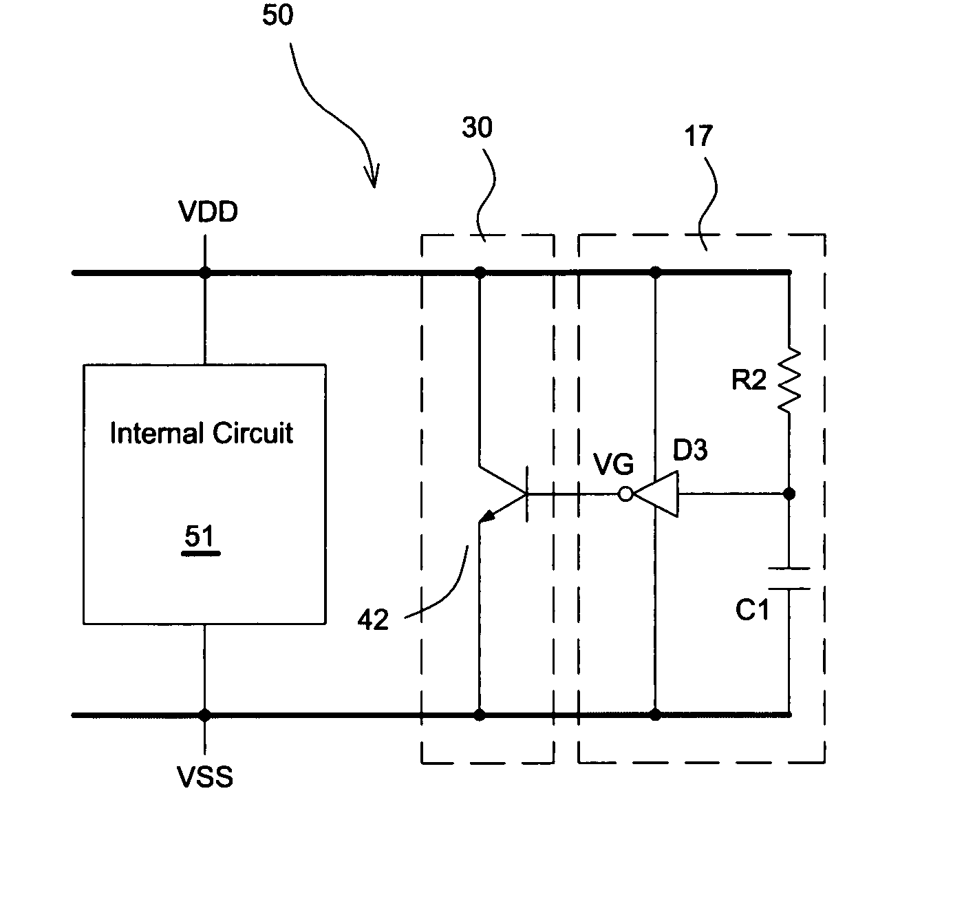
[0024]FIG. 3 illustrates an embodiment of an ESD clamp circuit having a deep N-well structure of the invention. Referring to FIG. 3, the ESD clamp circuit 50 of the invention includes a discharge circuit 30 with a deep N-well structure and an ESD detecting unit 17. In the embodiment, the discharge circuit 30 and the ESD detecting unit 17 are applied to an integrated circuit chip and are coupled between a first voltage VDD and a second voltage VSS so as to protect an internal circuit 51 from the ESD damage. The first voltage VDD is positive and the second voltage VSS is ground or negative in this embodiment. The discharge circuit 30 provides a path for the electrostatic discharge so as to bypass the electrostatic charge current when the electrostatic charges surges over the integrated circuit chip. The ESD detecting unit 17 detects the voltage difference between the first voltage VDD and second voltage VSS and generates a trigger signal VG for the discharge circuit 30. Because the ES...


PUM


Abstract

An ESD clamp circuit includes an ESD detecting unit and a discharge circuit with a longitudinal BJT. The longitudinal BJT is formed on a P-type substrate and includes a deep N-well formed on the P-type substrate, a P-well formed on parts of the deep N-well, a N-well formed on the deep N-well surrounding the P-well, a first N+ region formed on parts of the P-well and electrically coupled to a first voltage, a P+ region formed on the P-well surrounding the first N+ region and electrically coupled to a trigger signal, and a second N+ region formed on the N-well and electrically coupled to a second voltage. In the structure of the longitudinal BJT, the leakage current can be decreased, the current gain can be increased, and the dimension of the ESD clamp circuit can be reduced.

Description

[0001] This application claims the benefit of Taiwan application Serial No. 092118102, filed Jul. 2, 2003. BACKGROUND OF THE INVENTION [0002] 1. Field of the Invention [0003] The invention relates to an ElectroStatic Discharge (hereinafter called ESD) clamp circuit, and more particularly to an ESD clamp circuit using a deep N-well structure to form a longitudinal BJT (bipolar junction transistor) for electrostatic discharge. [0004] 2. Description of the Related Art [0005] In order to constitute a high circuit-integration density and achieve desired functions, a metal-oxide-semiconductor field-effect transistor (MOSFET) with reduced size has been used in the advanced integrated circuit (IC) technology. However, in order to satisfy the demand of the constant field scaling, a power supply voltage is also scaled down in some IC technology. Hence, the computer architecture needs an interface to connect semiconductor chips or sub-systems having different power supply voltages. Owing to th...

Claims


Application Information

Patent Timeline
Patent Type & Authority Applications(United States)
IPC IPC(8): H01L23/60H01L27/02H01L27/082H02H9/08
CPCH01L27/0259H01L2924/0002H01L2924/00
Inventor YEH, TA-HSUNLEE, CHAO-CHENGTSAUR, TAY-HER
Owner REALTEK SEMICON CORP
Why Eureka
Try Eureka