
Method for fabricating a semiconductor memory having charge trapping memory cells and semiconductor substrate

a technology of charge trapping memory cells and semiconductor substrates, which is applied in the direction of semiconductor devices, instruments, electrical equipment, etc., can solve the problems of inability to fast access memory contents and inability to optimize memory transistors, and achieve the effect of better contras

Inactive Publication Date: 2005-01-06
POLARIS INNOVATIONS
View PDF8 Cites 1 Cited by
  • Summary
  • Abstract
  • Description
  • Claims
  • Application Information

AI Technical Summary

Benefits of technology

[0009] This method has the advantage that, in the region of the remaining portions of the electrically conductive material, in particular of the cross-connections, the electrical insulation at the lateral walls of the word lines is not attached as a result of contact holes being etched out, into which contact holes the electrically conductive material is subsequently introduced in each case. Dielectric spacers provided at the sidewalls of the word lines thus retain their initial thickness, thereby ensuring a sufficient electrical insulation between the word lines and the rest of the electrically conductive material. In this way, the top-side bit lines and the special arrangement of the transistor structures that is formed by the cross-connections can be fabricated in a simple manner. The memory cells can thereby be packed very densely in a memory cell array

Problems solved by technology

This results in various difficulties: the memory transistors cannot be optimized by a precise setting of the source / drain dopings.
The word lines have a small cross section, so that fast access to the memory contents is not possible owing to the low electrical conductivity caused as a result of said small cross section.

Method used


Image

  • Method for fabricating a semiconductor memory having charge trapping memory cells and semiconductor substrate
  • Method for fabricating a semiconductor memory having charge trapping memory cells and semiconductor substrate
  • Method for fabricating a semiconductor memory having charge trapping memory cells and semiconductor substrate

Examples


Embodiment Construction

[0017] The making and using of the presently preferred embodiments are discussed in detail below. It should be appreciated, however, that the present invention provides many applicable inventive concepts that can be embodied in a wide variety of specific contexts. The specific embodiments discussed are merely illustrative of specific ways to make and use the invention, and do not limit the scope of the invention.

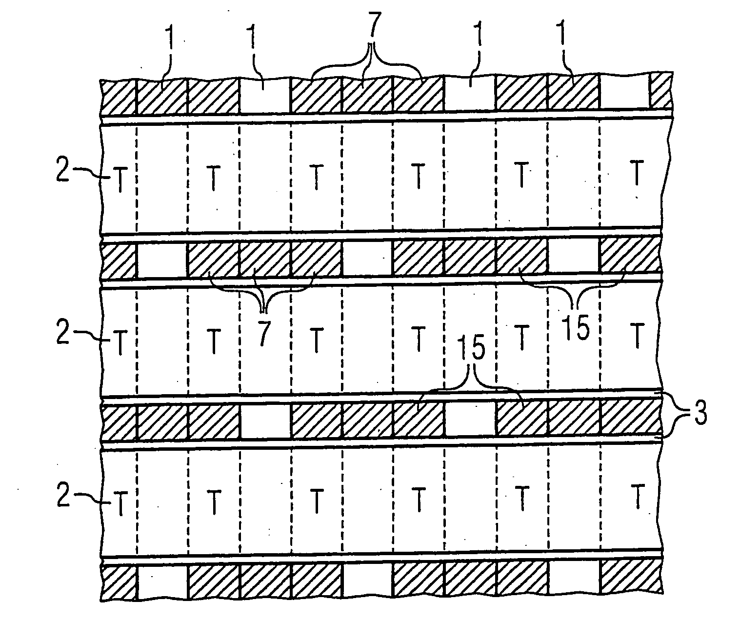
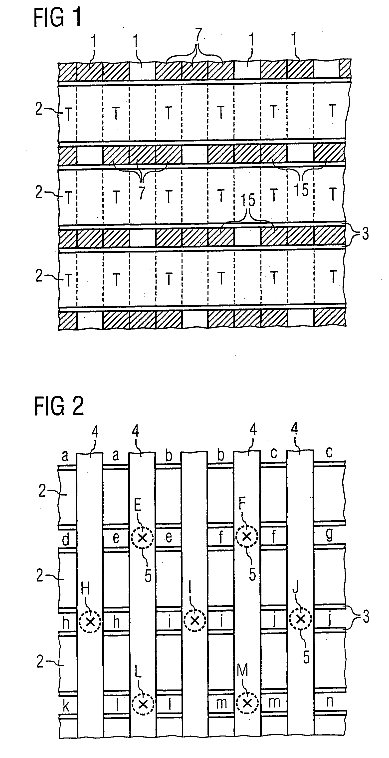
[0018]FIG. 1 shows, for an exemplary embodiment, a plan view of a scheme revealing the positions of the STI isolations 1, word lines 2 with lateral spacers 3 and the regions that are to be electrically conductively connected to one another. The STI isolations 1 (shallow trench isolation) are isolation trenches which are arranged parallel at a distance from one another and filled with dielectric and between which there are, in each case, channel regions of the transistors T that run parallel to the isolation trenches below each word line 2. The word lines 2 therefore, run ov...


PUM


Abstract

Electrically conductive material is introduced into interspaces between the word lines (2) and is partially removed using a mask (6) in such a way that residual portions (7) of the conductive material in each case fill a section of the relevant interspace and produce an electrical contact with source / drain regions (15). With further portions of the conductive material, it is possible to form alignment marks for the fabrication process.

Description

TECHNICAL FIELD [0001] The present invention relates generally to semiconductor devices and methods and more particularly to a method for fabricating a semiconductor memory having charge trapping memory cells. BACKGROUND [0002] Charge trapping memory cells, such as planar SONOS memory cells or NROM memory cells are discussed in U.S. Pat. Nos. 5,768,192 and 6,011,725 or International Publication No. WO 99 / 60631. These devices have an oxide-nitride-oxide storage layer sequence as gate dielectric and are programmed by channel hot electrons (CHE) and erased by hot holes. A virtual ground array comprising NROM cells is usually provided with word lines which run above the source / drain regions and cross with buried bit lines. The transistor current therefore flows parallel to the word lines. This results in various difficulties: the memory transistors cannot be optimized by a precise setting of the source / drain dopings. The word lines have a small cross section, so that fast access to the ...

Claims


Application Information

Patent Timeline
Patent Type & Authority Applications(United States)
IPC IPC(8): H10B20/00H10B69/00H10B99/00
CPCH01L27/11568H01L27/115H10B43/30H10B69/00
Inventor KRAUSE, MATHIASLUDWIG, CHRISTOPHSACHSE, JENS-UWEDEPPE, JOACHIMRICHTER, RALFKLEINT, CHRISTOPHMIKALO, RICARDO
Owner POLARIS INNOVATIONS
Features
  • Generate Ideas
  • Intellectual Property
  • Life Sciences
  • Materials
  • Tech Scout
  • Unparalleled Data Quality
  • Higher Quality Content
  • 60% Fewer Hallucinations
Learn More