Thin film resistor etch

a resistor etching and thin film technology, applied in the field of thin film resistor etching, can solve the problems that analog precision and mixed signal devices have not been fabricated using these submicron densities, and achieve the effect of enhancing the low pressure environment and reducing the damage associated

Inactive Publication Date: 2005-01-06
TEXAS INSTR INC
View PDF14 Cites 18 Cited by
  • Summary
  • Abstract
  • Description
  • Claims
  • Application Information

AI Technical Summary

Problems solved by technology

Conventionally, analog precision and mixed signal devices have not been fabricated employing these submicron densities.

Method used


Image

  • Thin film resistor etch
  • Thin film resistor etch
  • Thin film resistor etch

Examples


Embodiment Construction

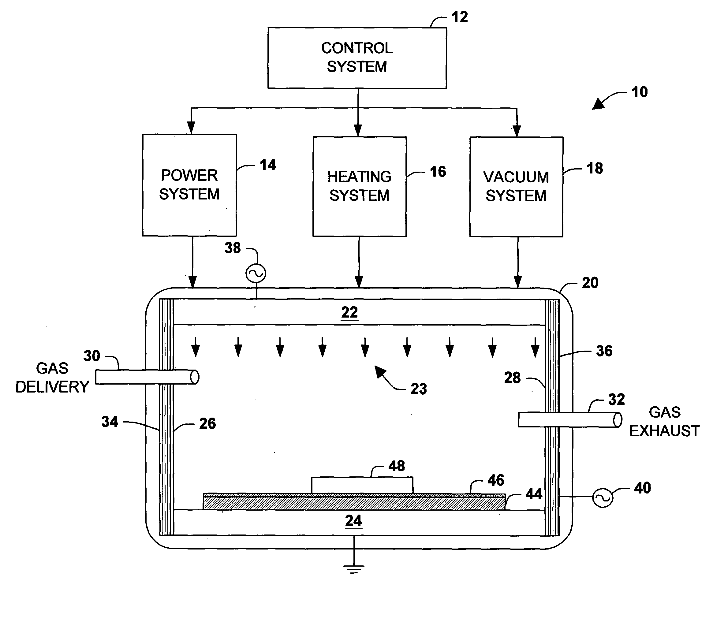
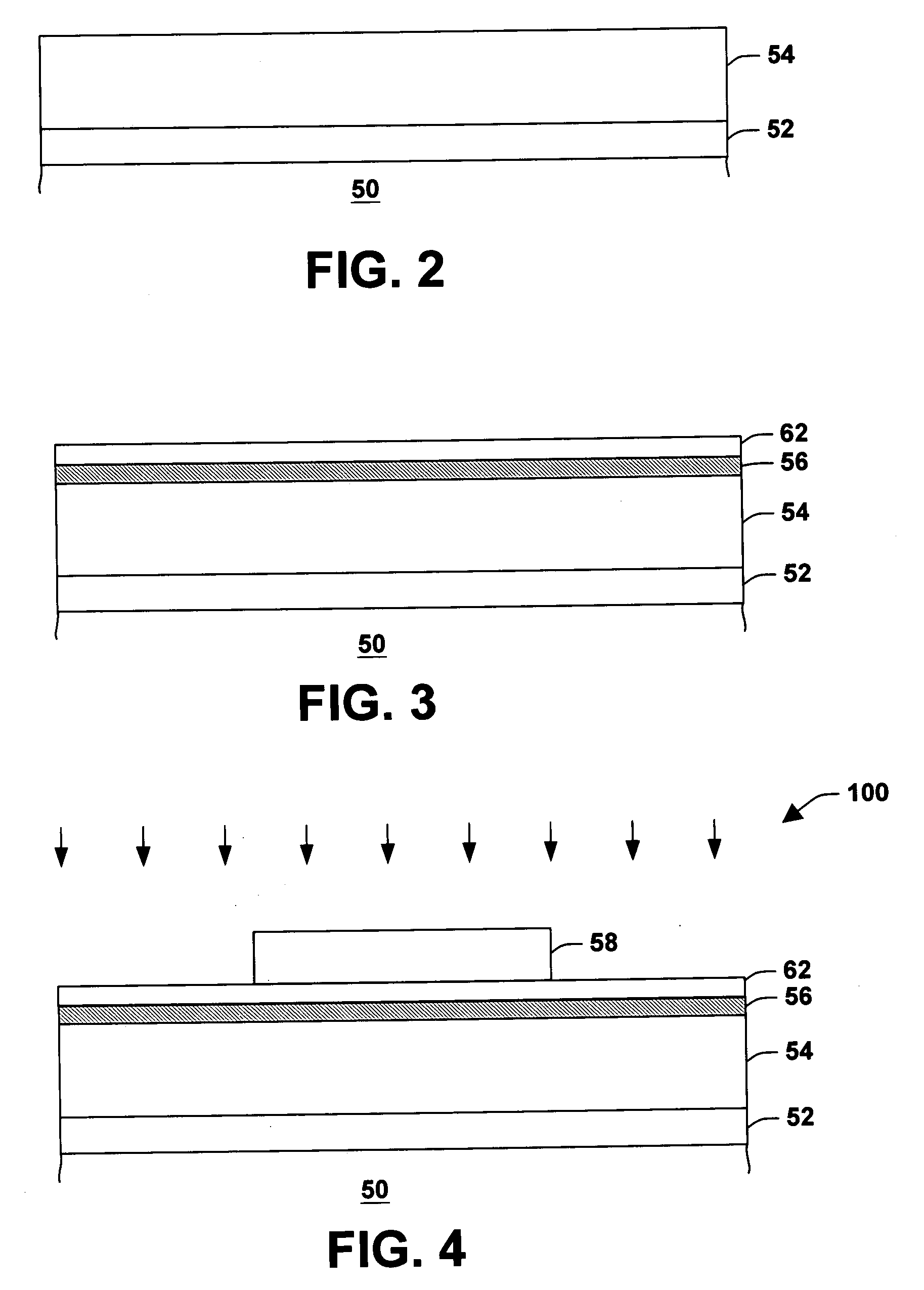
[0024] The present invention relates to the formation of a TFR by employing a plasma etch on a resistor material layer formed of a nickel chromium (NiCr) alloy, or nickel chromium aluminum (NiCrAl) alloy. The plasma etch can be performed in a magnetically enhanced (e.g., in a magnetic field) low pressure (e.g., at or below 30 mTorr) environment with a chlorine and boron tri-chloride plasma chemistry mixture. The plasma etch mitigates resist adhesion issues associated with wet etch processes. The plasma etch also mitigates resistor width issues associated with resistor designs in addition to reducing the costs associated with employing wet etch chemistries versus plasma process gases.

[0025] Conventionally, a NiCr or NiCrAl resistor is formed by etching a NiCr or NiCrAl resistor material layer over a dielectric layer. A patterned photoresist layer is then provided over the resistor material layer to form the pattern for the thin film resistor. A wet etch having a nickel soluble compo...


PUM

PropertyMeasurementUnit
pressureaaaaaaaaaa
poweraaaaaaaaaa
temperatureaaaaaaaaaa

Abstract

A thin film resistor is formed by employing a plasma etch on a resistor material layer. The resistor material layer can be fabricated employing a nickel chromium (NiCr) alloy, or nickel chromium aluminum (NiCrAl) alloy. A plasma etch is performed in a magnetically enhanced low pressure environment with a chlorine chemistry mixture. The magnetically enhanced low pressure environment and the sufficiently selective chlorine chemistry provide a substantially controlled plasma etch of the resistor material layer to form the thin film resistor. In-situ thickness measurements or an endpoint optical emission system can be employed to determine when to halt the etching process to mitigate damage associated with etching of the layer underlying the thin film resistor.

Description

TECHNICAL FIELD [0001] The present invention relates to semiconductor devices and, more particularly, to a thin film resistor etch. BACKGROUND OF THE INVENTION [0002] In the semiconductor industry, there is a continuing trend toward higher device densities. To achieve these high densities, there has been and continues to be efforts toward scaling down device dimensions to submicron levels (e.g., below 0.35 microns) on semiconductor substrates. In order to accomplish such high device packing density, smaller and smaller features sizes are required. This may include the width and spacing of metal interconnecting lines, spacing and diameter of contact holes, and the surface geometry such as corners and edges of various features. Conventionally, analog precision and mixed signal devices have not been fabricated employing these submicron densities. This is because the precision of the analog devices and the selection of available materials for precision analog devices have been overridin...

Claims


Application Information

Patent Timeline
Patent Type & Authority Applications(United States)
IPC IPC(8): C23F4/00H01L21/02H01L21/302H01L21/3213H01L21/461
CPCB81C99/0065B81C2201/0138H01L28/24H01J37/32082H01L21/32136C23F4/00
Inventor MAHDAVI, OMID
Owner TEXAS INSTR INC
Why Eureka
Try Eureka