

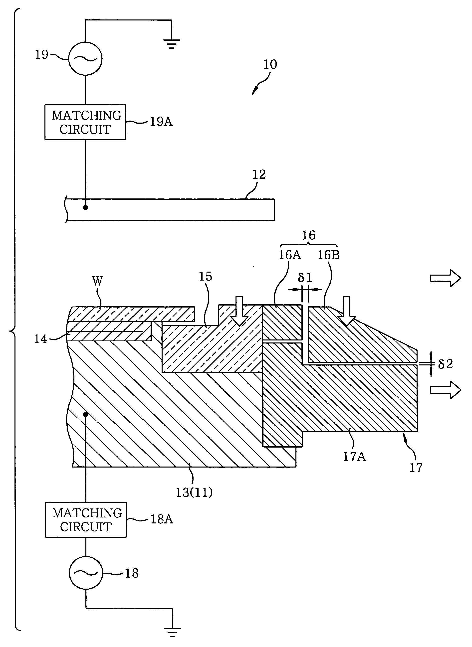
Ring mechanism, and plasma processing device using the ring mechanism
a plasma processing device and ring mechanism technology, applied in the direction of coatings, chemical vapor deposition coatings, electric discharge tubes, etc., can solve the problem of potential difference between, deterioration of line width over the entire surface of the wafer, and the likelihood of an exposure of the surface covered by the mask
- Summary
- Abstract
- Description
- Claims
- Application Information
AI Technical Summary
Benefits of technology
Problems solved by technology
Method used
Image

Examples
verification example 1
First, as shown in FIGS. 12A to 12E, five types of inner rings 25, 64, 65, 66 and 67 (the inner rings 65 to 67 do not have a protruded portion) were prepared and etching was conducted under the same processing condition for each case. Then, uniformity of etching processing was inspected.
<Experimental Conditions for Verification>
The type in FIG. 12A (experimental example 1) shows an inner ring 25 of a type described in the foregoing preferred embodiments, wherein a length a and a thickness of the planar surface portion 48 was 20 mm and 6.5 mm, respectively; and the thickness of the protruded portion 49 was 7.5 mm.
The type in FIG. 12B (experimental example 2) illustrates an inner ring 64 which is identical to that of the experimental example 1 with an exception of the length of the planar surface portion 48 which was 10 mm.
The type in FIG. 12C (comparative example 1) shows a flat inner ring 65 having a thickness of 65 mm and the surface of the inner ring 65 is substantiall...
verification example 2
<Experimental Conditions for Verification>
In this verification example, inner rings and outer rings of types illustrated in FIGS. 16A, 16B and FIGS. 17A and 17B were prepared, and etching was conducted under the same processing condition for each case. Then, uniformity of etching process was inspected.
The type in FIG. 16A (experimental example 3) shows an inner ring 25 of a type described in the first preferred embodiment, wherein the length a and the thickness of a planar surface portion 48 was 20 mm and 6.5 mm, respectively; the thickness of a protruded portion 49 was 7.5 mm; and the height of the top surface of an outer ring 26 was set to be lower than that of the top surface of the protruded portion 49 by 1 mm.
The type in FIG. 16B (comparative example 4) illustrates an inner ring 25 identical to that employed in the experimental example 3, wherein the height of the top surface of an outer ring 68 is set to be substantially identical to that of the top surface of a prot...
experimental example 1
A. Experimental Condition
The plasma processing device shown in FIG. 22 was employed. Six types were prepared by setting the width c of the first ring 91, which ranges from the inner peripheral portion defined as 0 to the outer peripheral portion thereof, to be 7.5 mm, 17.5 mm, 22.5 mm, 25 mm, 30 mm and 40 mm, respectively. The pressure of four types was set to be 15 mTorr, 25 mTorr, 35 mTorr and 50 mTorr for each condition, respectively. Further, bias powers corresponding to the outer diameters a2 were set to be 1400 W, 1550 W, 1585 W, 1650 W, 1800 W and 1950 W, respectively, in order to uniformly maintain an even bias power per unit area in the inner region rather than in the outer peripheral portion of the first ring 91.
B. Experimental Result
In each sample, etching rates of 16 spots in the region within 10 mm from the peripheral portion of the wafer W were inspected and, at the same time, etching rates of 21 spots in the region inner than corresponding region were inspected...
PUM
| Property | Measurement | Unit |
|---|---|---|
| Length | aaaaa | aaaaa |
| Length | aaaaa | aaaaa |
| Fraction | aaaaa | aaaaa |
Abstract
Description
Claims
Application Information