Eureka AIR delivers breakthrough ideas for toughest innovation challenges, trusted by R&D personnel around the world.

Circuit assembly having compliant substrate structures for mounting circuit devices

a technology of circuit devices and substrates, applied in the field of substrates, can solve problems such as fatigue cracking of smd, and achieve the effect of reducing thermally induced stresses in the device, without sacrificing reliability

Inactive Publication Date: 2005-01-13
DELPHI TECH INC
View PDF7 Cites 7 Cited by
  • Summary
  • Abstract
  • Description
  • Claims
  • Application Information

AI Technical Summary

Benefits of technology

[0009] The present invention is directed to a circuit assembly comprising a substrate formed to have one or more apertures that define one or more compliant members in the substrate, and to which a circuit device can be attached so as to reduce thermally-induced stresses in the device and in solder joints securing the device to the substrate. The compliant members are sufficiently compliant to permit relatively large surface-mount devices to be attached to an organic substrate without sacrificing reliability.
[0010] Generally, the circuit assembly of this invention includes the substrate and a surface-mount device mounted thereto, multiple electrically-conductive pads present on at least one device attachment region of the substrate, and solder joints bonding the surface-mount device to the pads. The entire substrate, including the device attachment region and a second region outside the device attachment region, can be formed of a first material, e.g., an organic. The surface-mount device comprises a package (chip) formed of a material (e.g., silicon or a ceramic) having a lower coefficient of thermal expansion than the substrate material. At least one aperture is formed in the substrate, and is located and configured so as to cause the device attachment region (or at least a portion thereof) to be more compliant than the second region of the substrate, though both are formed of the same material. In this manner, the surface-mount device, mounted to the substrate through the pads located within a compliant region of the device attachment region, is subjected to lower thermally-induced stresses as compared to mounting the surface-mount device to the second (and less compliant) region of the substrate.
[0011] In view of the above, the present invention enables large surface-mount devices (SMD's) to be placed on organic substrates (circuit boards), though a significant CTE mismatch exists between the organic substrate and SMD. More particularly, the compliant region(s) to which the SMD is attached reduces thermally-induced stresses that lead to fatigue fracturing of the solder joints that attach the SMD to the substrate and can also lead to fatigue cracking of the SMD. Accordingly, the processing and packaging advantages associated with large SMD's can be achieved on organic (e.g., FR4, Chem 1, Chem 3, etc.) circuit boards, even when service temperatures are about 100° C. or higher.

Problems solved by technology

More particularly, the compliant region(s) to which the SMD is attached reduces thermally-induced stresses that lead to fatigue fracturing of the solder joints that attach the SMD to the substrate and can also lead to fatigue cracking of the SMD.

Method used


Image

  • Circuit assembly having compliant substrate structures for mounting circuit devices
  • Circuit assembly having compliant substrate structures for mounting circuit devices
  • Circuit assembly having compliant substrate structures for mounting circuit devices

Examples


Embodiment Construction

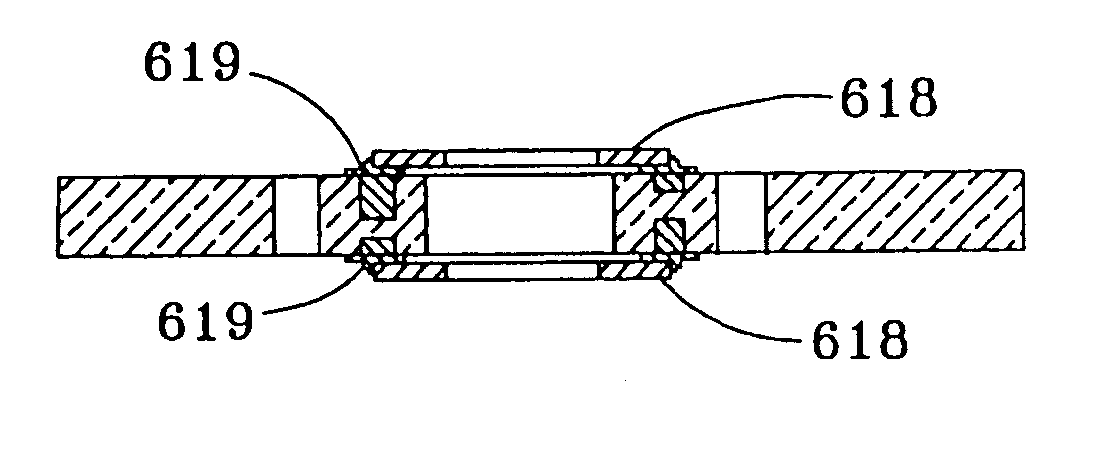
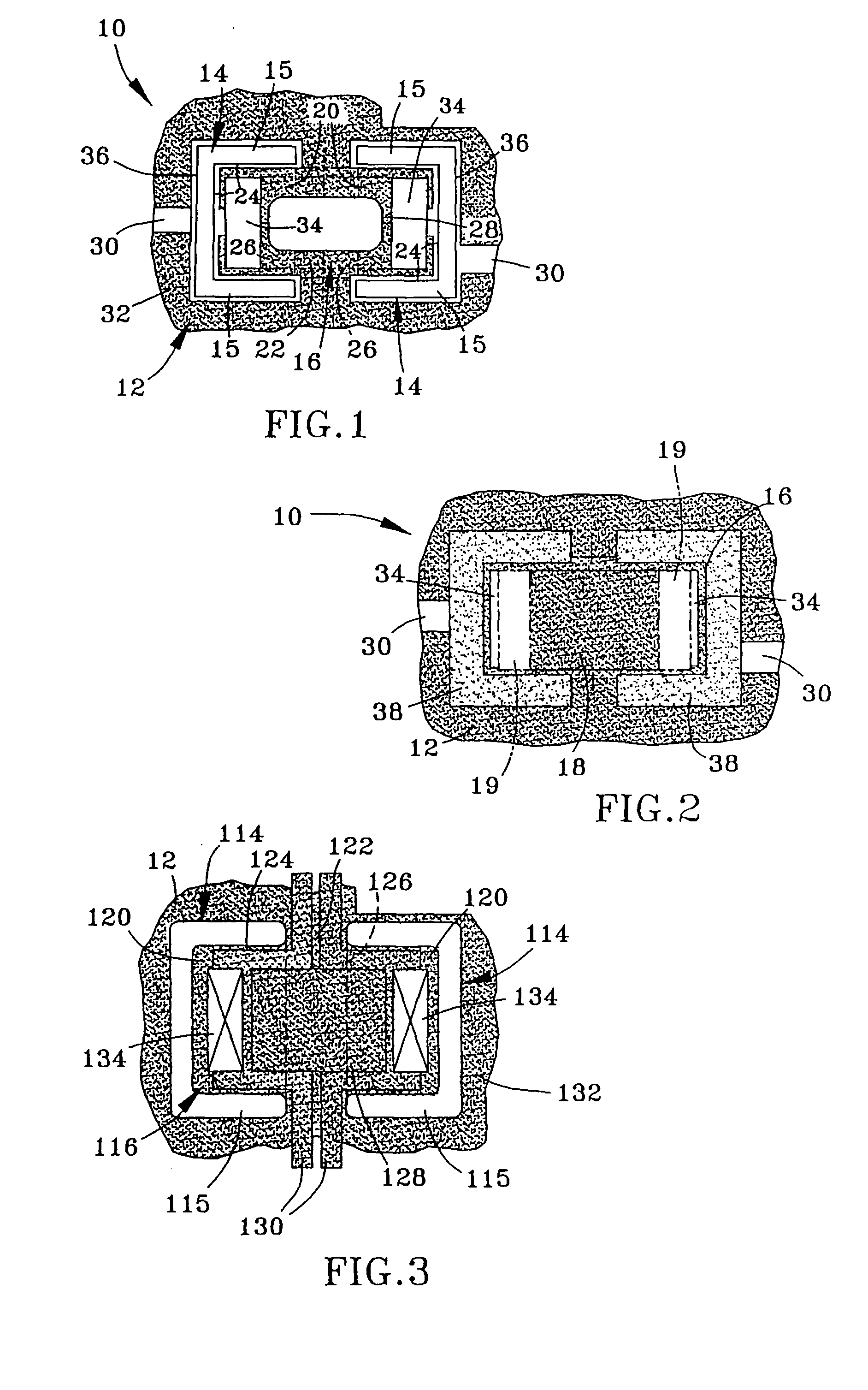
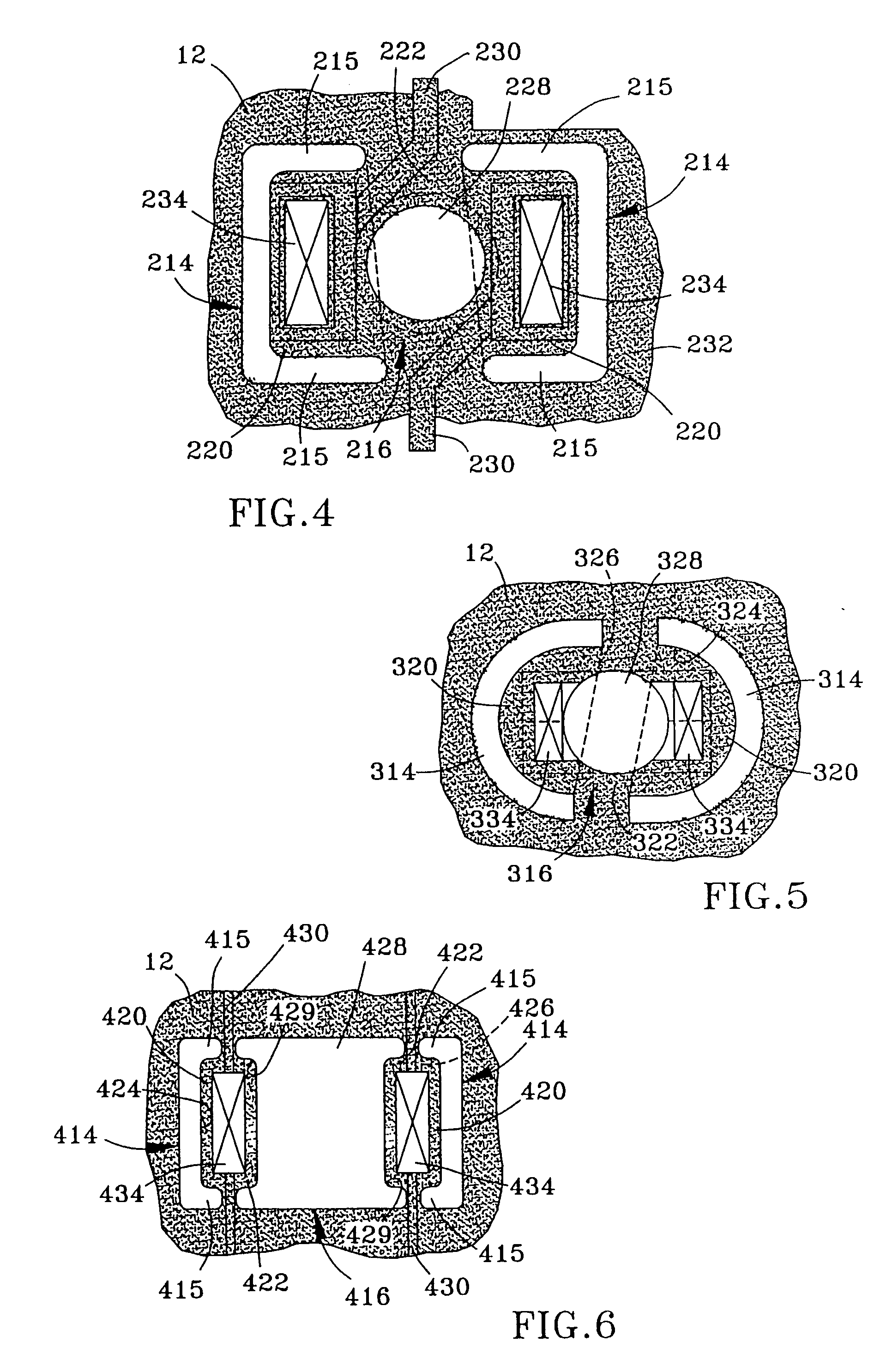
[0017]FIGS. 1 through 11 depict portions of a circuit assembly 10 with device attachment regions configured in accordance with various embodiments of the present invention, for the purpose of attaching surface-mount devices (SMD's) to a substrate, referred to herein as a circuit board 12. The SMD's can be of any type known or subsequently developed, though of particular interest to the invention are relatively large SMD's such as the 2512 chip (package or case form), with dimensions of about 6.5×3.25 mm. Furthermore, the circuit board 12 can be formed of a variety of materials, though of particular interest are circuit boards formed of organic materials, such as FR4, Chem 1, and Chem 2, which are generally glass-reinforced or woven fiberglass-reinforced epoxy resin laminate materials available from various commercial sources.

[0018]FIGS. 1 and 2 represent a first embodiment of this invention, in which a pair of substantially U-shaped slots (apertures) 14 with parallel sets of legs 1...


PUM


Abstract

A circuit assembly comprising a substrate formed to have one or more apertures that define one or more compliant members in the substrate, and to which a circuit device can be attached so as to reduce thermally-induced stresses in the device and in solder joints securing the device to the substrate. The compliant members are sufficiently compliant to permit relatively large surface-mount devices to be attached to an organic substrate without sacrificing reliability.

Description

CROSS REFERENCE TO RELATED APPLICATIONS [0001] Not applicable. STATEMENT REGARDING FEDERALLY SPONSORED RESEARCH [0002] Not applicable. BACKGROUND OF THE INVENTION [0003] (1) Field of the Invention [0004] The present invention generally relates to substrates on which circuit devices are mounted. More particularly, this invention relates to a circuit assembly having a substrate equipped with one or more compliant structures to which a circuit device can be attached so as to reduce thermally-induced stresses in the device and in the solder joints that secure the device to the substrate. [0005] (2) Description of the Related Art [0006] Surface-mount technology (SMT) offers the advantages of increased reliability and lower manufacturing costs. Surface-mount devices (SMD) used in SMT processes are available in a range of chip or die (package or case form) sizes, with larger SMD's including the 2512 chips (about 6.5×3.25 mm), diodes, inductors, capacitors, resistors, varisters, etc. In man...

Claims


Application Information

Patent Timeline
IPC IPC(8): H05K1/02H05K3/34
CPCH05K1/0271H05K3/326H05K3/3442H05K2201/10636H05K2201/09072H05K2201/09081H05K2201/09063Y02P70/50
Inventor STILLABOWER, MORRIS D.
Owner DELPHI TECH INC
Why Eureka
Eureka Blog
Learn More