Semiconductor memory device and method for fabricating the same

a memory device and semiconductor technology, applied in semiconductor devices, semiconductor/solid-state device details, electrical devices, etc., can solve the problems of difficult reduction of the size of each element, complicated process steps for integrating storage elements, and complicated steps for performing separate steps. to achieve the effect of reducing the size of the devi

Active Publication Date: 2005-01-13
TAIWAN SEMICON MFG CO LTD
View PDF5 Cites 65 Cited by
  • Summary
  • Abstract
  • Description
  • Claims
  • Application Information

AI Technical Summary

Benefits of technology

[0008] It is an object of the present invention to further improve, in a semiconductor memory device including a logic section and a memory section, consistency of processes for forming a memory section with a logic process and make it possible to reduce the size of the device.
[0009] A semiconductor memory device according to the present invention has a structure in which side and bottom surfaces of a storage element in a memory section is covered with a resistance heating element. This structure can be formed according to a logic process. Accordingly, process steps for fabricating a semiconductor memory device including a logic section and a memory section can be simplified, so that the number of fabrication process steps can be reduced as a whole. Moreover, the structure of the memory section is simplified. Therefore, size reduction and integration of elements become possible.
[0011] The resistance heating element and the storage element in this structure can be formed by a fabrication method including less fabrication process steps such as lithography and etching performed separately from a logic process, compared to the case of fabricating a known semiconductor memory device in which a resistance heating element film covers only a lower surface of a storage element film. Furthermore, the respective structures of a storage element film and a resistance heating film are simplified. Therefore, size reduction and integration of elements become possible.
[0018] In this method, compared to the case of forming the known semiconductor memory device in which a resistance heating element film covers only a lower surface of the storage element film, the number of process steps such as lithography and etching performed separately from a logic process can be reduced. Thus, process steps can be simplified. Furthermore, the respective structures of a storage element film and a resistance heating element film in a memory section are simplified. Therefore, size reduction and integration of elements become possible.
[0022] In this method, compared to the case of forming the known semiconductor memory device in which a resistance heating element film covers only a lower surface of the storage element film, the number of process steps such as lithography and etching performed separately from a logic process can be reduced. Thus, process steps can be simplified. Furthermore, the respective structures of a storage element film and a resistance heating element film in a memory section are simplified. Therefore, size reduction and integration of elements become possible.

Problems solved by technology

As has been described, in a known method, although it is possible to make some of the steps for fabricating a storage element have consistency with a logic process, a complicated step has to be performed separately from the logic process.
As has been described, process steps for integrating storage elements are complicated and make reduction in the size of each element difficult.

Method used


Image

  • Semiconductor memory device and method for fabricating the same
  • Semiconductor memory device and method for fabricating the same
  • Semiconductor memory device and method for fabricating the same

Examples


first embodiment

(First Embodiment)

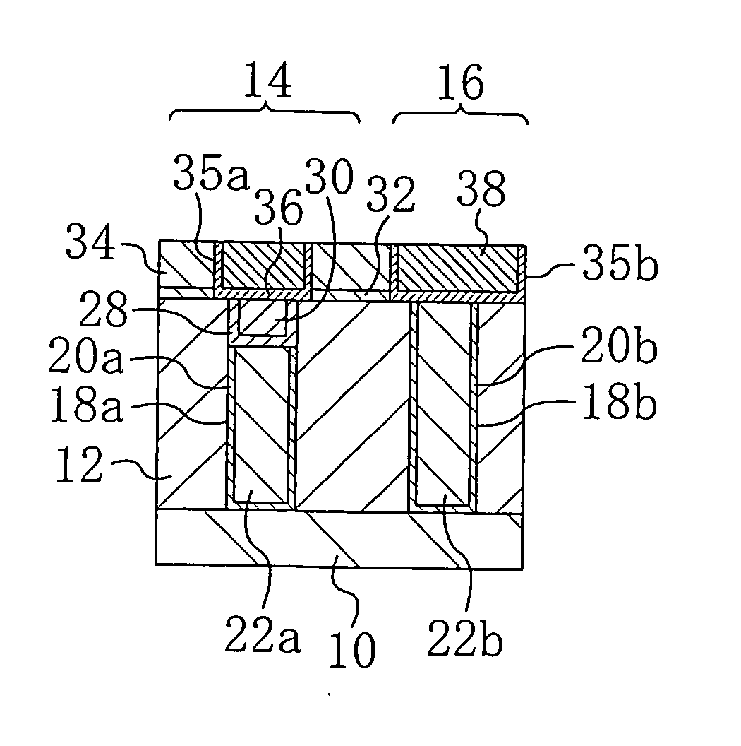
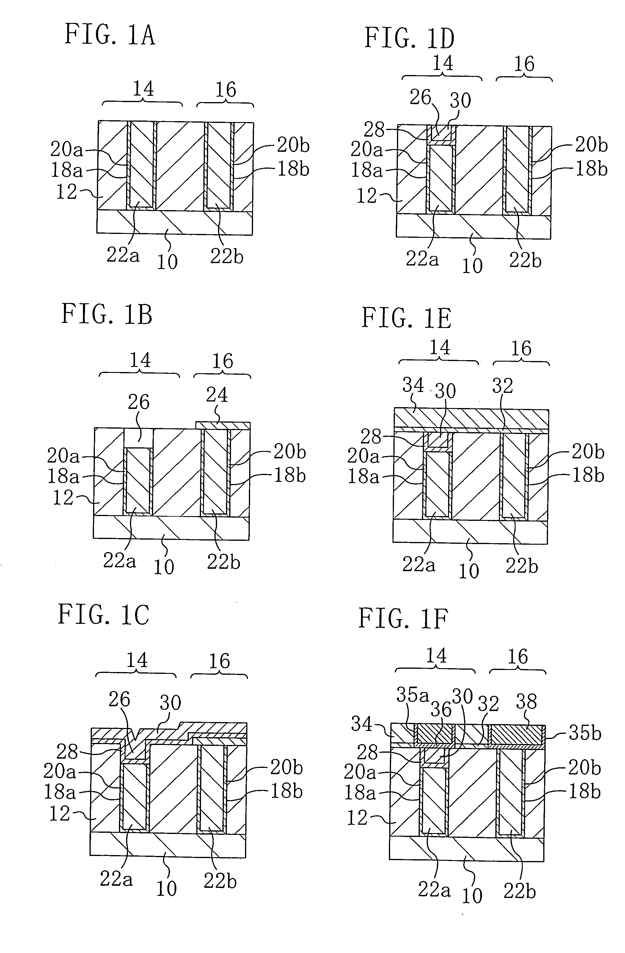
[0030] First, a method for fabricating a semiconductor memory device according to the present invention will be described with reference to FIGS. 1A through 1F. FIGS. 1A through 1F are cross-sectional views illustrating respective steps for fabricating a semiconductor memory device according to a first embodiment of the present invention.

[0031] In the method for fabricating a semiconductor memory device according to this embodiment, thermal CVD is first performed in the step of FIG. 1A, thereby forming a first insulating film 12 made of a phosphorus-doped oxide film and having a thickness of 0.8 μm on a 200 mm-diameter silicon substrate 10 on which elements (not shown) are provided. Thereafter, to flat levels generated in an upper surface of the first insulating film 12 resulting from unevenness of an upper surface of the silicon substrate 10, etch back is performed using an inversion mask (not shown) and then flattening is further performed to the first insulatin...

second embodiment

(Second Embodiment)

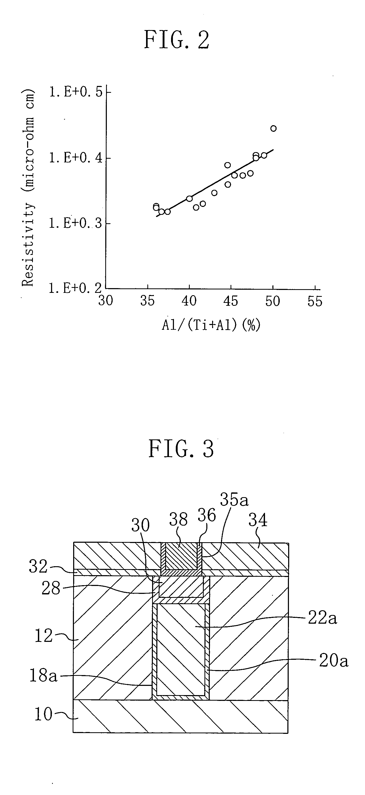
[0046] In this embodiment, the case where the resistance heating element film 28 and the storage element film 30, which are provided in the first insulating film 12 in the first embodiment, are provided in the second insulating film 34 will be described. FIGS. 4A through 4F are cross-sectional views illustrating respective steps for fabricating a semiconductor memory device according to a second embodiment of the present invention. In this embodiment, a first insulating film 12, contact holes 18a and 18b, adhesion layers 20a and 20b, and tungsten plugs 22a and 22b are first formed in the step of FIG. 4A in the same manner as in the step of FIG. 1A.

[0047] In the step of FIG. 4B, a first barrier film 32 made of SiC or SiN is deposited over the first insulating film 12 and the tungsten plugs 22a and 22b to a thickness of 50 nm by plasma CVD. Subsequently, a second insulating film 34 made of SiO2 or a SiOC film is deposited over the first barrier film 32 to a thickne...


PUM


Abstract

In a fabrication method according to the present invention, a first insulating film and tungsten plugs are formed over a substrate including a logic section and a memory section. An upper portion of one of the tungsten plug located in a memory section is removed, thereby forming a recess. A resistance heating element film covering side and bottom surfaces of the recess and a storage element film filling the recess with the resistance heating element film interposed between the storage element film and the plug are formed. Then, a Cu interconnect is formed on the storage element film. Thus, it is possible to make the process step of forming the resistance heating element film and the storage element film have higher consistency with a logic process.

Description

BACKGROUND OF THE INVENTION [0001] The present invention relates to a nonvolatile memory using resistance change accompanied with phase change and a method for fabricating the same. [0002] As a known semiconductor memory device using a chalcogenide material, for example, semiconductor memory device is disclosed in U.S. Pat. No. 6,236,059. FIG. 5 is a cross-sectional view of the known semiconductor memory device using a chalcogenide material disclosed in U.S. Pat. No. 6,236,059. [0003] Respective steps for fabricating a nonvolatile memory of FIG. 5 will be described. First, an interlayer insulating film 104 deposited over a silicon substrate 102 is patterned to form a contact hole 106 reaching the silicon substrate 102. Then, polysilicon (not shown) is deposited over the interlayer insulating film 104 by thermal CVD to fill the contact hole 106 and then part of polysilicon located on the interlevel insulating film 104 is removed by CMP. Thereafter, a recess is formed by selectively e...

Claims


Application Information

Patent Timeline
Patent Type & Authority Applications(United States)
IPC IPC(8): H01L21/3205H01L21/3065H01L21/768H01L23/52H01L27/10H01L27/105H01L29/76H01L45/00
CPCH01L45/06H01L45/1233H01L45/1683H01L45/144H01L45/126H10N70/8413H10N70/231H10N70/8828H10N70/826H10N70/066
Inventor OKUNO, YASUTOSHI
Owner TAIWAN SEMICON MFG CO LTD
Why Eureka
Try Eureka