Semiconductor device and driving method thereof

a technology of semiconductor devices and driving methods, applied in the direction of logic circuit coupling/interface arrangements, pulse techniques, instruments, etc., can solve problems such as problems such as problems in source driver circuits, current flowing to light emitting elements, and difficult realization of large and high definition displays

Inactive Publication Date: 2005-01-13
SEMICON ENERGY LAB CO LTD
View PDF16 Cites 27 Cited by
  • Summary
  • Abstract
  • Description
  • Claims
  • Application Information

AI Technical Summary

Benefits of technology

[0046] According to the invention, the precharge operation is performed before the set operation. Therefore, the set operation ca

Problems solved by technology

The former has a simple structure, but has a problem such that a realization of a large and high definition display is difficult.
In the case of a display device of the active matrix method, there is a problem that a current flowing to a light emitting element varies due t

Method used


Image

  • Semiconductor device and driving method thereof
  • Semiconductor device and driving method thereof
  • Semiconductor device and driving method thereof

Examples


embodiment

[0127] [Embodiment Mode 1]

[0128] The invention can be applied not only to a pixel having a light emitting element such as an EL element, but to various analog circuits having a current source. First, in this embodiment mode, a basic principle of the invention is described.

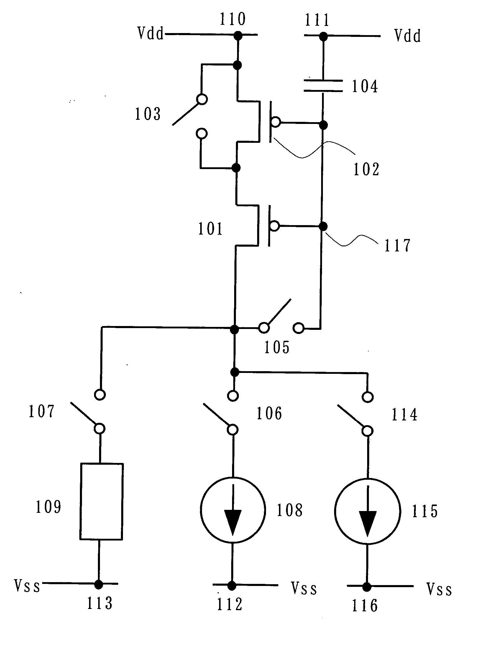
[0129] First, FIG. 1 shows a configuration of the current source circuit based on the basic principle of the invention. A current source transistor 101 which constantly operates as a current source (or a part of it) and a switching transistor 102 of which operation changes according to the circumstance of a circuit are provided, and the current source transistor 101, the switching transistor 102, and a wiring 110 are connected in series.

[0130] A gate terminal of the current source transistor 101 is connected to one terminal of a capacitor 104. The other terminal of the capacitor 104 is connected to a wiring 111. Therefore, it is possible to hold a potential of the gate terminal of the current source transistor 10...


PUM


Abstract

The invention provides a semiconductor device which performs a write operation of a signal current rapidly to a current input type pixel. Before inputting a signal current, a precharge operation is performed by flowing a large current. After that, a signal current is inputted to perform the set operation. A predetermined potential can be obtained rapidly as the precharge operation is performed before the set operation. The predetermined potential is approximately equal to a potential after completing the set operation. Therefore, the set operation can be rapidly performed and a write operation of a signal current can be rapidly performed. By using two transistors, a gate width W can be long or a gate length L can be short in the precharge operation or the gate width W can be short and the gate length L can be long in the set operation.

Description

TECHNICAL FIELD [0001] The present invention relates to a semiconductor device provided with a function to control by a transistor a current to be supplied to a load, and more particularly to a semiconductor device including a pixel formed of a current drive type light emitting element which changes its luminance according to a current, and a signal line driver circuit thereof. BACKGROUND ART [0002] In recent years, a self-luminous type display device of which pixel is formed of a light emitting element such as a light emitting diode (LED) is attracting attention. As a light emitting element used in such a self-luminous type display device, an organic light emitting diode (OLED), an organic EL element, and an electroluminescence (EL) element are attracting attention and becoming to be used in an organic EL display and the like. [0003] Being self-luminous type, such a light emitting element as an OLED has a high visibility of a pixel and provides a rapid response without a need of a ...

Claims


Application Information

Patent Timeline
IPC IPC(8): G09G3/20G09G3/30H03K3/00H03K17/00H03K17/693H05B33/14
CPCG09G3/325G09G2300/0809G09G2300/0842G09G2310/0251H03K17/687G09G2310/0275G09G2320/0223H03J2200/26G09G3/32G09G2310/0262G09G3/20G09G3/30H03K17/00H03K17/693G09G3/3233
Inventor KIMURA, HAJIME
Owner SEMICON ENERGY LAB CO LTD
Why Eureka
Try Eureka