Methods of manufacturing wiring pattern, organic electro luminescent element, color filter, plasma display panel, and liquid crystal display panel, and electronic apparatus

a technology of organic electro luminescent elements and manufacturing methods, which is applied in the manufacture of electrode systems, electric discharge tubes/lamps, instruments, etc., can solve the problems of low mass production efficiency, long time, and achieve low mass production efficiency , the effect of long time and reduced reliability of elements

Inactive Publication Date: 2005-01-13
SEIKO EPSON CORP
View PDF16 Cites 16 Cited by
  • Summary
  • Abstract
  • Description
  • Claims
  • Application Information

AI Technical Summary

Benefits of technology

[0007] A deposition method utilizing vacuum deposition or sputtering is implemented by batching and thus takes a long time such that mass production efficiency is low. Furthermore, in the case of a small molecule material, there is a problem that crystallization is easy to occur after deposition such that reliability o

Problems solved by technology

A deposition method utilizing vacuum deposition or sputtering is implemented by batching and thus takes a long time such that mass production efficiency is low.
Furthermore, in the case of a small molecule material, there is a problem that crystallization is easy to occur after deposition such that reliability of an element is decreased.
In a case where micro patterning is required when fabricating a full color display, there is a problem that high accuracy patterning is difficult in an evaporation method.
Endurance of materials is insufficient for a patterning process by photolithography.
The same pro

Method used


Image

  • Methods of manufacturing wiring pattern, organic electro luminescent element, color filter, plasma display panel, and liquid crystal display panel, and electronic apparatus
  • Methods of manufacturing wiring pattern, organic electro luminescent element, color filter, plasma display panel, and liquid crystal display panel, and electronic apparatus
  • Methods of manufacturing wiring pattern, organic electro luminescent element, color filter, plasma display panel, and liquid crystal display panel, and electronic apparatus

Examples


first exemplary embodiment

[0068] First Exemplary Embodiment

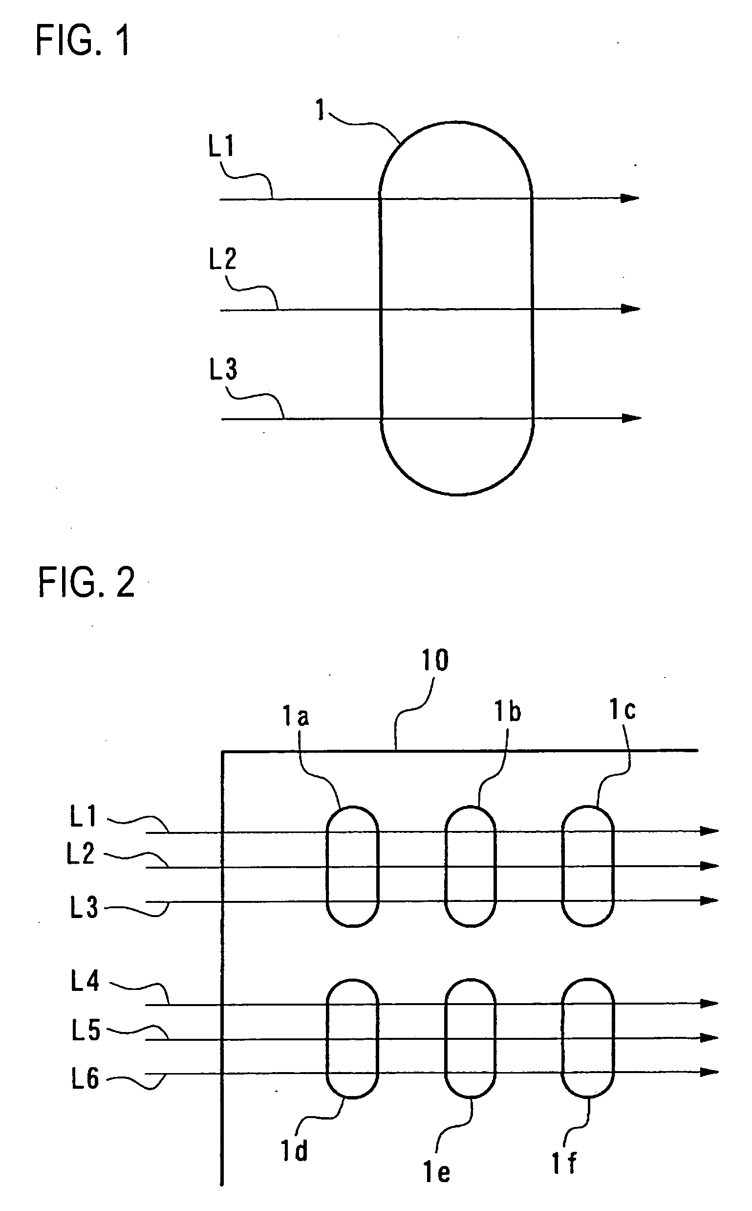
[0069]FIG. 1 is a schematic showing a method of manufacturing a thin film pattern according to a first exemplary embodiment of the invention. The pixel area 1 is formed on a substrate. Convex partition walls (banks) may be provided on the circumference of the pixel area 1. The pixel area 1 has an elongated shape, and has a major axis that passes through the center of the pixel area 1 and goes through the pixel area 1 longitudinally, and a minor axis that passes through the center of the pixel area 1 and transverses the pixel area 1. The shape of the pixel area 1 may be rectangle, oval, or the like.

[0070] A liquid material is applied to the pixel area 1 by a droplet ejecting method. In the case where a pixel formed in the pixel area 1 is an organic EL element for example, the liquid material includes a material that forms a hole injection layer or a light emitting layer and a solvent. Scanning lines L1, L2, and L3, shown in FIG. 1, are scanning lines...

second exemplary embodiment

[0088] Second Exemplary Embodiment

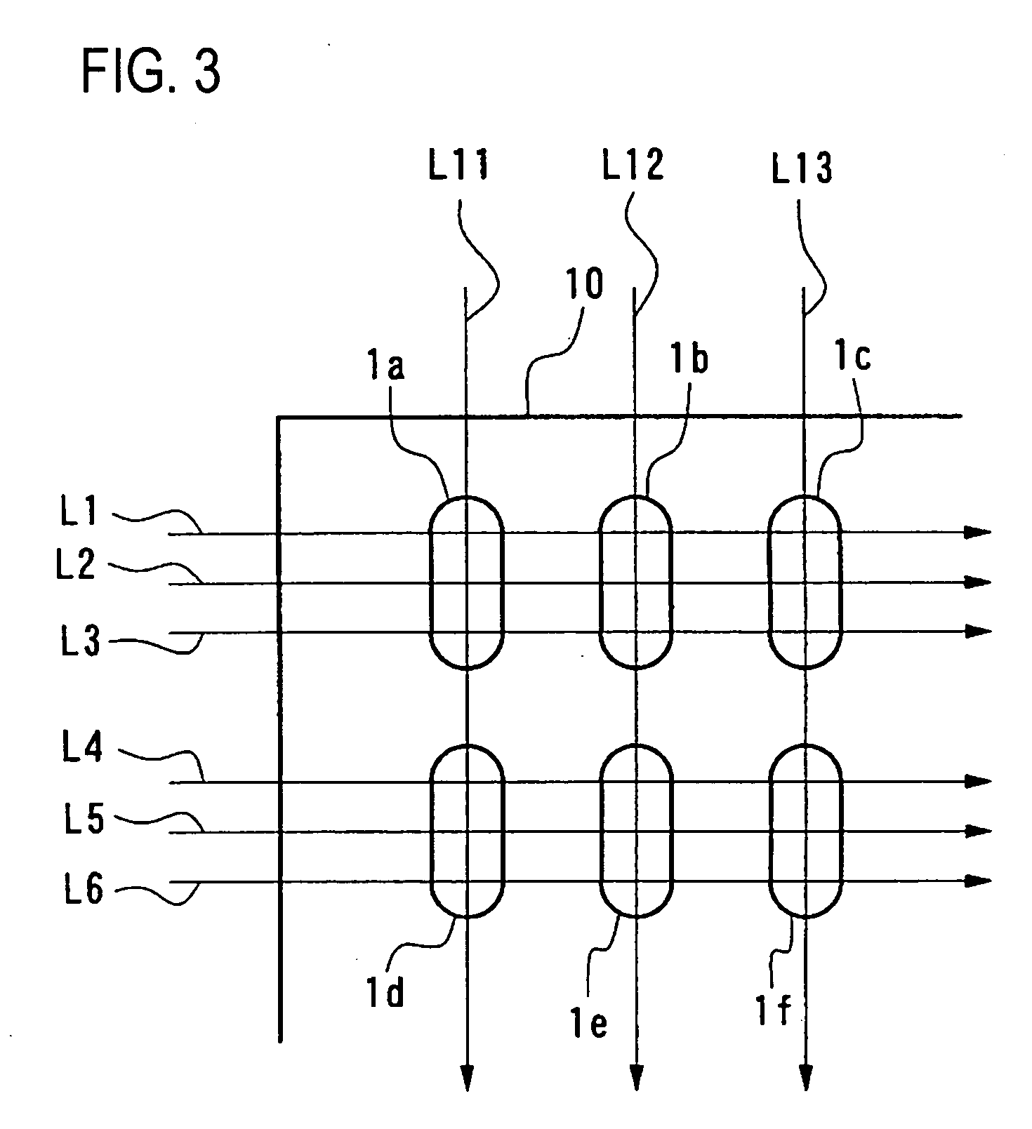
[0089] A second exemplary embodiment of the present invention will be described referring to FIG. 3. FIG. 3 is a schematic showing a method of manufacturing a thin film pattern according to a second exemplary embodiment of the invention. The second exemplary embodiment is different from the first exemplary embodiment in that not only the scanning lines L1, L2, L3, L4, L5, and L6 are arranged along the minor axis direction of the pixel areas 1a, 1b, 1c, 1d, 1e, and 1f but also scanning lines L11, L12, and L13 are arranged along the major axis direction of the pixel areas 1a, 1b, 1c, 1d, 1e, and 1f.

[0090] Specifically, the plurality of pixel areas 1a, 1b, 1c, 1d, 1e, and 1f are formed on a top surface of the substrate 10. Convex partition walls (banks) may be provided on the circumference of each of the pixel areas 1a, 1b, 1c, 1d, 1e, and 1f.

[0091] The scanning lines L1, L2, and L3 are arranged for the pixel areas 1a, 1b, and 1c formed as pixels of ...

third exemplary embodiment

[0095] Third Exemplary Embodiment

[0096] A third exemplary embodiment of the present invention will be described referring to FIGS. 4 and 5. FIG. 4 is a schematic showing a method of manufacturing a thin film pattern according to a third exemplary embodiment of the invention. In the exemplary embodiment, a droplet ejecting apparatus where a plurality of inkjet nozzles 21a, 21b, and 21c are formed in a nozzle head 20 is used. Each of the inkjet nozzles 21a, 21b, and 21cmay be disposed at a certain interval on a certain straight line in the nozzle head 20.

[0097] For the pixel area 1, the plurality of scanning lines L1, L2, and L3 are arranged in parallel with the minor axis of the pixel area 1. Then, the nozzle head 20 is moved along the minor axis direction of the pixel area 1 so that the inkjet nozzle 21a moves above the scanning line L1, the inkjet nozzle 21b above the scanning line L2, and the inkjet nozzle 21c above the scanning line L3.

[0098] Here, the nozzle head 20 is moved s...


PUM


Abstract

Methods of manufacturing a thin film pattern, an organic electro-luminescent element, a color filter, a plasma display panel, and a liquid crystal display panel, and an electronic apparatus in which the generation of streak unevenness in a thin film pattern can be reduced or prevented or the streak unevenness can be dispersed are provided when the thin film pattern constituting a pixel is formed using a droplet ejecting method. A liquid applying treatment where a liquid material is applied to a pixel area having a major axis and a minor axis by a droplet ejecting method, and an ejecting treatment along minor axis direction where, in the liquid applying treatment, a nozzle head of a droplet ejecting apparatus is scanned along a minor axis direction of the pixel area (a direction of scanning lines L1, L2, and L3), and a droplet is ejected to the pixel area from an inkjet nozzle included in the nozzle head in the scanning process.

Description

BACKGROUND OF THE INVENTION [0001] 1. Field of Invention [0002] The present invention relates to methods of manufacturing a thin film pattern, an organic electro-luminescent device, a color filter, a plasma display panel, and a liquid crystal display panel in which a droplet ejecting method is used, and an electronic apparatus. [0003] 2. Description of Related Art [0004] A display panel using an organic electro-luminescent element has been contrived in the related art. A basic structure of an organic electro-luminescent element is formed by interposing a solid-state thin film (light emitting layer) including fluorescent organic molecules between two electrodes (cathode and anode). When voltage is applied to the electrodes, holes from the anode and electrons from the cathode are injected into the light emitting layer and thus fluorescence is emitted from the light emitting layer. [0005] A single layer structure element including only a light emitting layer has low light emitting effi...

Claims


Application Information

Patent Timeline
IPC IPC(8): B05D1/26G02F1/13G02F1/1335H01J9/02H01J9/24G02B5/20H01J11/12H01J11/22H01J11/24H01J11/26H01J11/34H01L51/00H01L51/40H01L51/50H01L51/56H05B33/10
CPCH01J9/02H01J9/205H01L51/56H01J2217/49207H01L51/0005H01J9/245H10K71/135H10K71/00G02F1/13
Inventor SAKAI, HIROFUMI
Owner SEIKO EPSON CORP
Why Eureka
Try Eureka