Semiconductor chip production method, semiconductor device production method, semiconductor chip, and semiconductor device

a semiconductor chip and semiconductor technology, applied in the direction of bridges, bridge structural details, basic electric elements, etc., can solve the problems of deteriorating the characteristics of the semiconductor chip, inconvenience in assembling the semiconductor chip into the semiconductor device, and the inability of the semiconductor chip to be properly connected to each other or to the wiring board, so as to achieve the effect of less susceptible to metal contamination

Active Publication Date: 2005-01-13
ROHM CO LTD
View PDF3 Cites 50 Cited by
  • Summary
  • Abstract
  • Description
  • Claims
  • Application Information

AI Technical Summary

Benefits of technology

[0025] It is an object of the present invention to provide a semiconductor chip w

Problems solved by technology

This results in contamination of the wafer W with copper of the metal material 106, thereby deteriorating the characteristics of the semiconductor chips.
When the semiconductor chips each having a smaller thickness are stacked to be assembled into a semico

Method used


Image

  • Semiconductor chip production method, semiconductor device production method, semiconductor chip, and semiconductor device
  • Semiconductor chip production method, semiconductor device production method, semiconductor chip, and semiconductor device
  • Semiconductor chip production method, semiconductor device production method, semiconductor chip, and semiconductor device

Examples


first embodiment

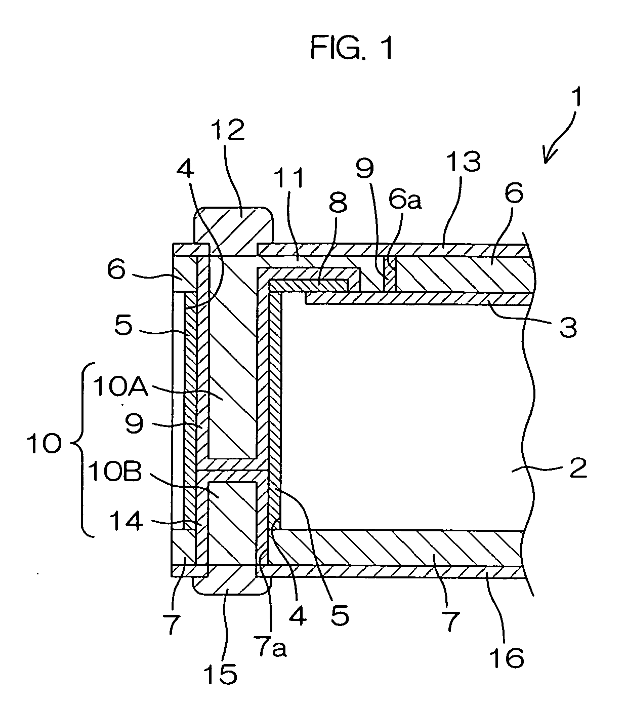
[0087]FIG. 1 is a schematic sectional view illustrating the construction of a semiconductor chip according to the present invention.

[0088] The semiconductor chip 1 includes a semiconductor substrate 2 of silicon. The semiconductor substrate 2 (semiconductor chip 1) has a thickness of about 100 μm. A functional device 3 having a plurality of electrodes are provided in one surface (hereinafter referred to as “front surface”) of the semiconductor substrate 2. A through-hole 4 extending thicknesswise through the semiconductor substrate 2 is provided on a lateral side of the functional device 3. An insulation film 5 of silicon oxide (SiO2) is provided on an inner peripheral surface of the through-hole 4.

[0089] A hard mask 6 having an opening 6a is provided on the front surface of the semiconductor substrate 2. The hard mask 6 is composed of silicon oxide. A part of the functional device 3 and the through-hole 4 are present in the opening 6a.

[0090] An insulation film 8 having a pattern ...

second embodiment

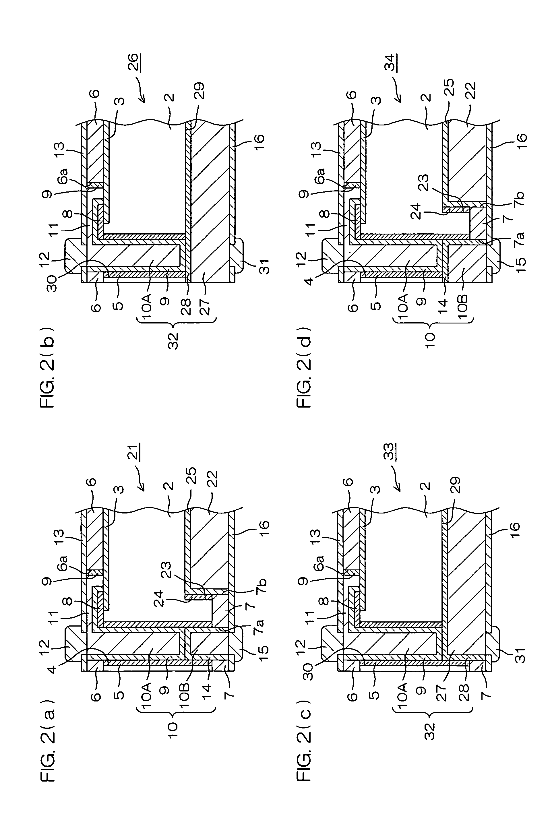
[0102] FIGS. 2(a) to 2(d) are schematic sectional views illustrating the constructions of semiconductor chips according to the present invention. In FIGS. 2(a) to 2(d), components corresponding to those shown in FIG. 1 are denoted by the same reference characters as in FIG. 1, and no explanation will be given thereto. These semiconductor chips 21, 26, 33, 34 each include a ground (earth) interconnection 22, 27 provided on the rear surface of the semiconductor substrate 2.

[0103] In the semiconductor chip 21 shown in FIG. 2(a), the semiconductor substrate 2 has a grounding recess 23 provided in the rear surface thereof on a lateral side of the through-hole 4. An insulation film 24 is provided on a side wall of the grounding recess 23. The hard mask 7 has an opening 7b in addition to the opening 7a. The opening 7b is generally aligned with the grounding recess 23 along the thickness of the semiconductor substrate 2.

[0104] A rear side seed layer 25 of copper is provided on interior sur...

third embodiment

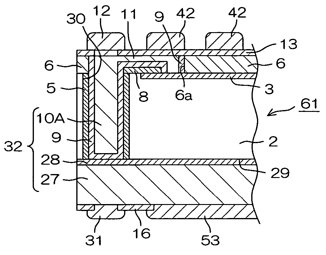
[0132] FIGS. 6(a) to 6(d) are schematic sectional views illustrating the constructions of semiconductor chips according to the present invention. In FIGS. 6(a) to 6(d), components corresponding to those shown in FIGS. 1 and 2(a) to 2(d) are denoted by the same reference characters as in FIGS. 1 and 2(a) to 2(d), and no explanation will be given thereto.

[0133] In the semiconductor chips 41, 44, 45, 46, the ground interconnection 22, 27 is provided on the rear surface of the semiconductor substrate 2. One or more dummy bumps 42, 43 (two dummy bumps 42 and two dummy bumps 43 in this embodiment) having no electrical connection are provided in addition to the bumps 12, 15, 31 on front and rear surfaces of the semiconductor chip 41, 44, 45, 46.

[0134] The dummy bumps 42 and the dummy bumps 43 are metal projections having substantially the same size and shape as the bump 12 and the bump 15, 31, respectively. The bump 12 and the dummy bumps 42 have substantially the same height, and the bum...


PUM


Abstract

A semiconductor chip production method including the steps of: forming a front side recess in a semiconductor substrate; depositing a metal material in the front side recess to form a front side electrode electrically connected to a functional device formed on the front surface; removing a rear surface portion of the semiconductor substrate to reduce the thickness of the semiconductor substrate to a thickness greater than the depth of the front side recess; forming a rear side recess communicating with the front side recess in the rear surface of the semiconductor substrate after the thickness reducing step; and depositing a metal material in the rear side recess to form a rear side electrode electrically connected to the front side electrode for formation of a through-electrode.

Description

BACKGROUND OF THE INVENTION [0001] 1. Field of the Invention [0002] The present invention relates to a semiconductor chip having a through-electrode extending thicknesswise therethrough and a production method for the semiconductor chip, and to a semiconductor device including a plurality of semiconductor chips stacked one on another and each having a through-electrode extending thicknesswise therethrough and a production method for the semiconductor device. [0003] 2. Description of Related Art [0004] A multichip module (MCM) is conventionally known as a semiconductor device which includes a plurality of semiconductor chips. In the conventional multichip module, the plurality of semiconductor chips are arranged on an insulative wiring board horizontally parallel to the wiring board. In this case, the multichip module has a greater footprint, i.e., takes a greater area when the multichip module is mounted on a second wiring board. [0005] In this connection, an attempt is made to redu...

Claims


Application Information

Patent Timeline
IPC IPC(8): H01L21/3205H01L21/60H01L21/768H01L23/52H01L23/12H01L23/31H01L23/48H01L25/065H01L25/07H01L25/18
CPCH01L21/76898H01L23/3128H01L2924/014H01L2924/01024H01L2924/01019H01L2924/01006H01L2924/01005H01L24/48H01L2924/15311H01L2924/01082H01L2924/01079H01L23/481H01L24/11H01L25/0657H01L25/50H01L2224/13099H01L2224/16145H01L2224/48091H01L2224/48227H01L2224/48465H01L2225/06513H01L2225/06517H01L2225/06541H01L2225/06586H01L2924/01004H01L2924/01013H01L2924/01022H01L2924/01029H01L2924/01033H01L2924/01049H01L2924/01074H01L2924/01075H01L2924/01078H01L2924/00014H01L2924/00H01L2224/451H01L2224/06181H01L2224/14181H01L2224/02372H01L2224/13025H01L2924/181H01L2224/45099E01D19/12E01D2101/28
Inventor TANIDA, KAZUMASANEMOTO, YOSHIHIKOTANAKA, NAOTAKA
Owner ROHM CO LTD
Why Eureka
Try Eureka