Direct patterning of silicon by photoelectrochemical etching

a technology of photoelectrochemical etching and direct patterning, which is applied in the direction of electric/magnetic computing, instruments, analogue processes for specific applications, etc., to achieve the effect of complex detail and high resolution

Active Publication Date: 2005-01-13
RGT UNIV OF CALIFORNIA
View PDF7 Cites 52 Cited by
  • Summary
  • Abstract
  • Description
  • Claims
  • Application Information

AI Technical Summary

Benefits of technology

[0007] The invention is directed to methods for direct patterning of silicon. The invention provides the ability to fabricate complex surfaces in silicon with three-dimensional features of high resolution and complex detail. The invention is suitable, for example, for use in soft lithography as embodiments of the invention can quickly create a master for use in soft lithog

Problems solved by technology

This makes the process generally suitable for small ar

Method used


Image

  • Direct patterning of silicon by photoelectrochemical etching
  • Direct patterning of silicon by photoelectrochemical etching

Examples


Embodiment Construction

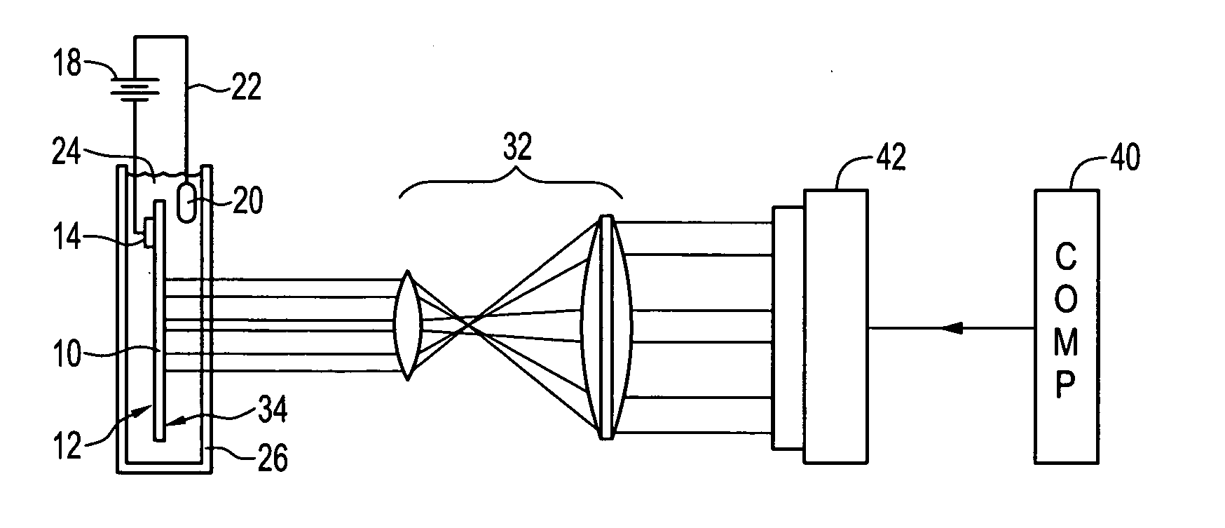
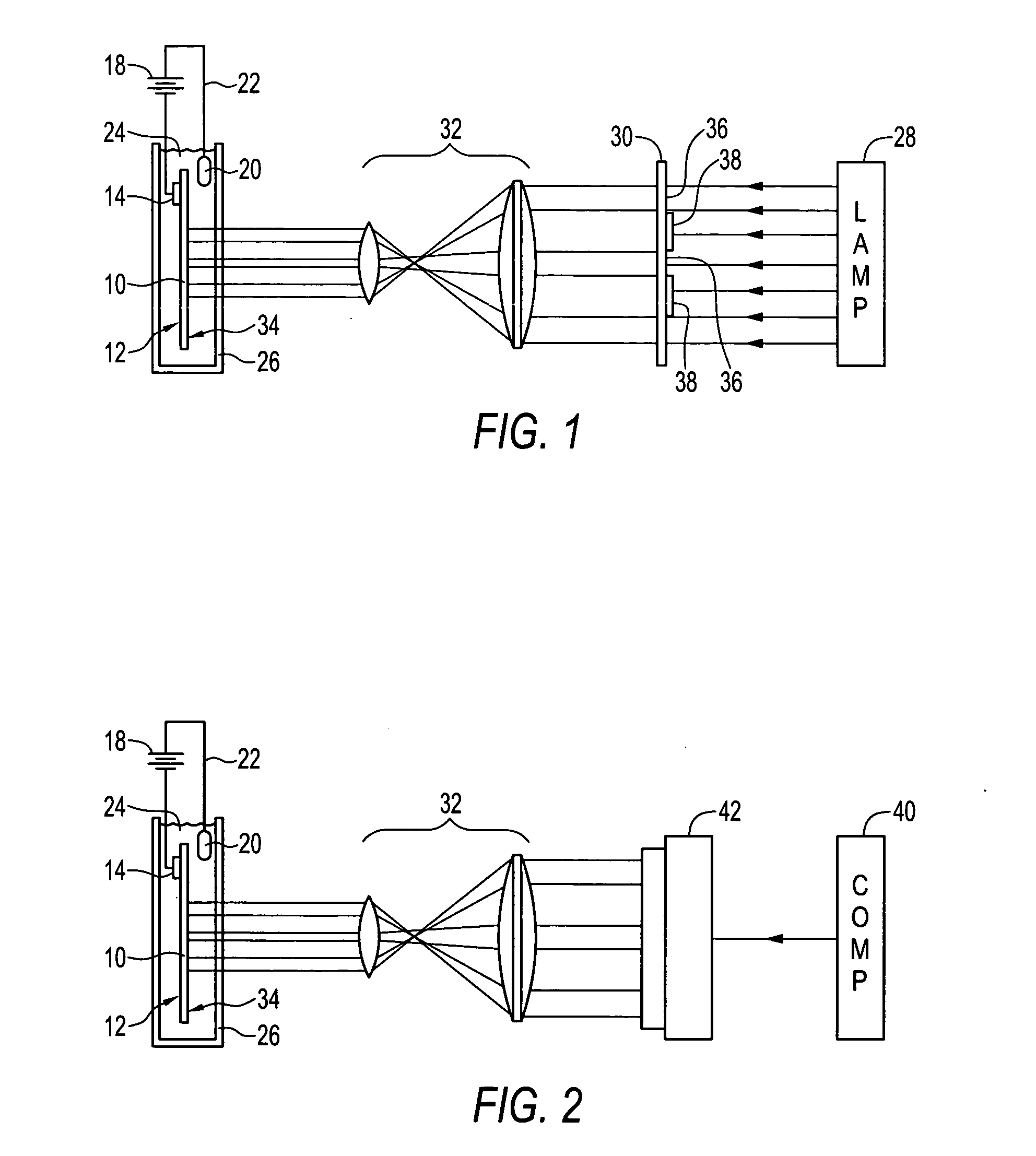
[0010] The invention is directed to methods for direct patterning of silicon. The invention provides the ability to fabricate complex surfaces in silicon with three-dimensional features of high resolution and complex detail. The invention is suitable, for example, for use in soft lithography as embodiments of the invention can quickly create a master for use in soft lithography.

[0011] In an embodiment of the invention for directly generating a three-dimensional pattern, a substrate having a silicon surface is selected. A first electrical conductor is affixed to the substrate for carrying a first charge to a backside of the substrate. A second electrical conductor for carrying a second charge opposite the first charge is selected, and immersed into a hydrofluoric acid-containing solution along with the substrate. An image is projected onto the silicon surface while current is applied to the first conductor and the second conductor to obtain an appropriate charge density. Afterwards,...


PUM

PropertyMeasurementUnit
Molar densityaaaaaaaaaa
Current densityaaaaaaaaaa
Interferenceaaaaaaaaaa

Abstract

The invention is directed to methods for direct patterning of silicon. The invention provides the ability to fabricate complex surfaces in silicon with three dimensional features of high resolution and complex detail. The invention is suitable, for example, for use in soft lithography as embodiments of the invention can quickly create a master for use in soft lithography. In an embodiment of the invention, electrochemical etching of silicon, such as a silicon wafer, for example, is conducted while at least a portion of the silicon surface is exposed to an optical pattern. The etching creates porous silicon in the substrate, and removal of the porous silicon layer leaves a three-dimensional structure correlating to the optical pattern.

Description

STATEMENT OF GOVERNMENT INTEREST [0001] The invention was made with Government assistance under Space and Naval War Systems Grant No. N6001-98-C-8514. The Government has certain rights in this invention.FIELD OF THE INVENTION [0002] The invention relates to the field of resistless optical lithography on silicon. The invention enables large-area, variable-depth images or patterns to be etched, in a single step, onto a silicon wafer with micrometer resolution. The invention is suitable, for example, for rapid prototyping of masters for use in soft lithography. A wide array of fields, such as sensors, microfluidics, microanalysis, microelectromechanical systems (MEMS) and cell biology might benefit from this invention. BACKGROUND [0003] Patterning of semiconductor wafers is usually carried out using photoresist masks patterned using UV light, electron beams or X-rays. There is recent interest in newer techniques for fabricating micro- or nanostructures. Many of the new techniques do no...

Claims


Application Information

Patent Timeline
IPC IPC(8): B81C1/00C25F3/12C25F3/14H01L21/26H01L21/3063
CPCC25F3/12C25F3/14B81C2201/0115B81C1/00515B81C2201/0114H01L21/3063
Inventor GAO, JUNSAILOR, MICHAEL J.BHATIA, SANGEETAFLAIM, CHRISTOPHER
Owner RGT UNIV OF CALIFORNIA
Why Eureka
Try Eureka