Plasma process apparatus and its processor

a processing apparatus and processing technology, applied in the field ofplasma processing apparatus and processing apparatus, can solve the problems of difficult effective optimization difficult effective improvement of microwave propagation efficiency within the dielectric member, and achieve the effect of improving the utilization efficiency of microwaves at the time of processing utilizing microwaves in the processing chamber, reducing the number of processing steps, and increasing the transmission efficiency of microwaves in the dielectric member

Inactive Publication Date: 2005-01-20
SHARP KK +1
View PDF10 Cites 15 Cited by
  • Summary
  • Abstract
  • Description
  • Claims
  • Application Information

AI Technical Summary

Benefits of technology

With this configuration, transmission efficiency of the microwaves in the dielectric member can be made sufficiently high. As such, the microwaves can be introduced into the processing chamber via the dielectric member more efficiently than conventional even if a microwave generator having performance of a conventional level is employed. As a result, it is readily possible to generate plasma under the condition that a pressure of a reactant gas for generating plasma within the processing chamber is decreased than conventional (i.e., under the condition where plasma generation would conventionally be difficult). Further, since the transmission efficiency of the microwaves in the dielectric member is improved, plasma can be generated in the processing chamber even if power of the microwaves propagating in the dielectric member is reduced than conventional. Accordingly, it is possible to widen the range of process conditions for plasma generation, such as the gas pressure and the microwave power, compared to the conventional case.
This configuration can considerably improve the transmission efficiency of the microwaves in the dielectric member.

Problems solved by technology

One of the most critical issues for the plasma processing apparatus of this kind is to improve uniformity and controllability of the process, or, to improve uniformity and controllability of the plasma.
The conventional techniques described above, however, pose the following problems.
It is considered that it would be difficult to effectively optimize the propagation efficiency of the microwaves with the technique disclosed in Japanese Patent Laying-Open No. 8-315998 that gives no consideration to the above-described points.
It is thus considered that there would be cases where it is difficult to effectively improve the propagation efficiency of the microwaves within the dielectric member.

Method used


Image

  • Plasma process apparatus and its processor
  • Plasma process apparatus and its processor
  • Plasma process apparatus and its processor

Examples


first embodiment

(First Embodiment)

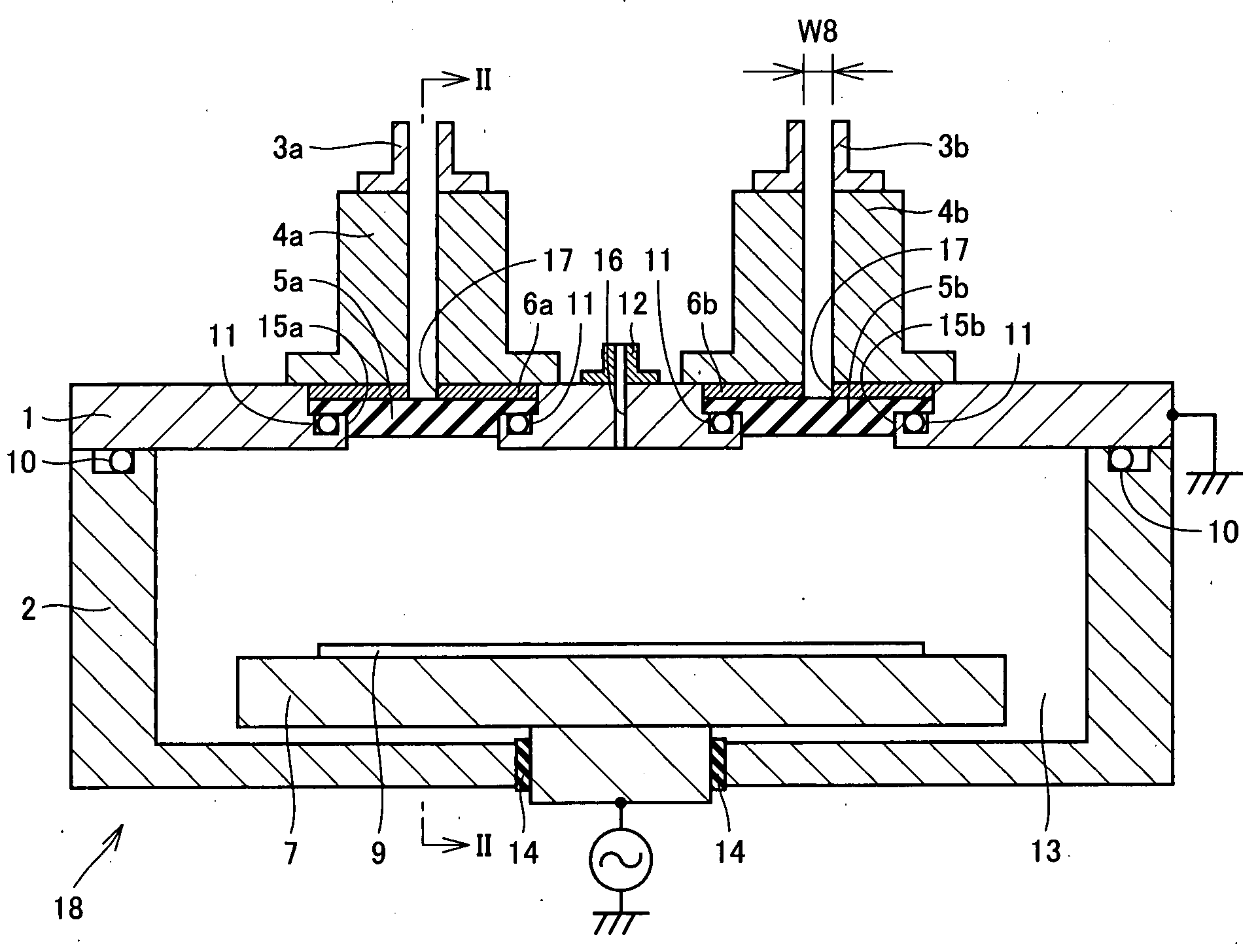
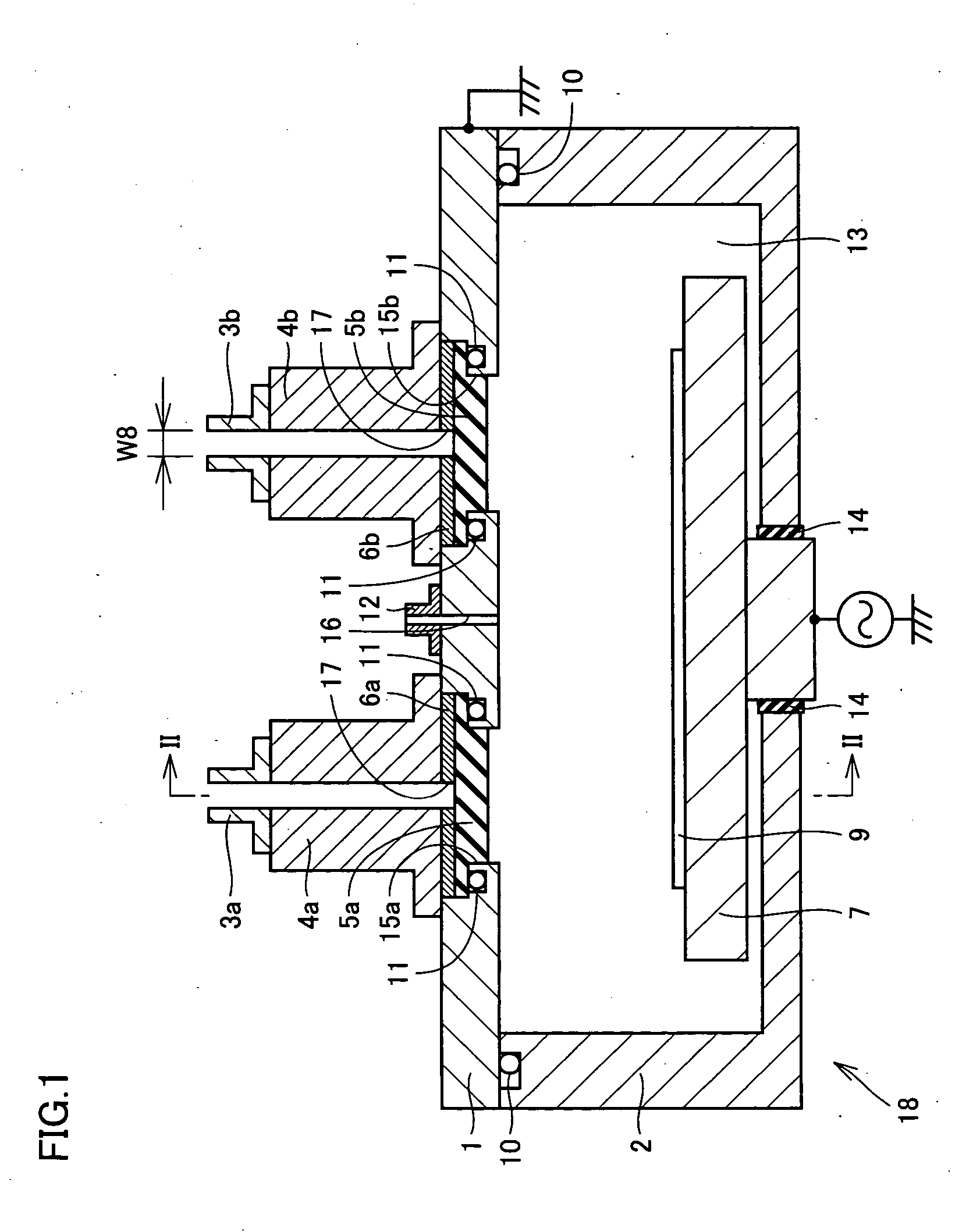
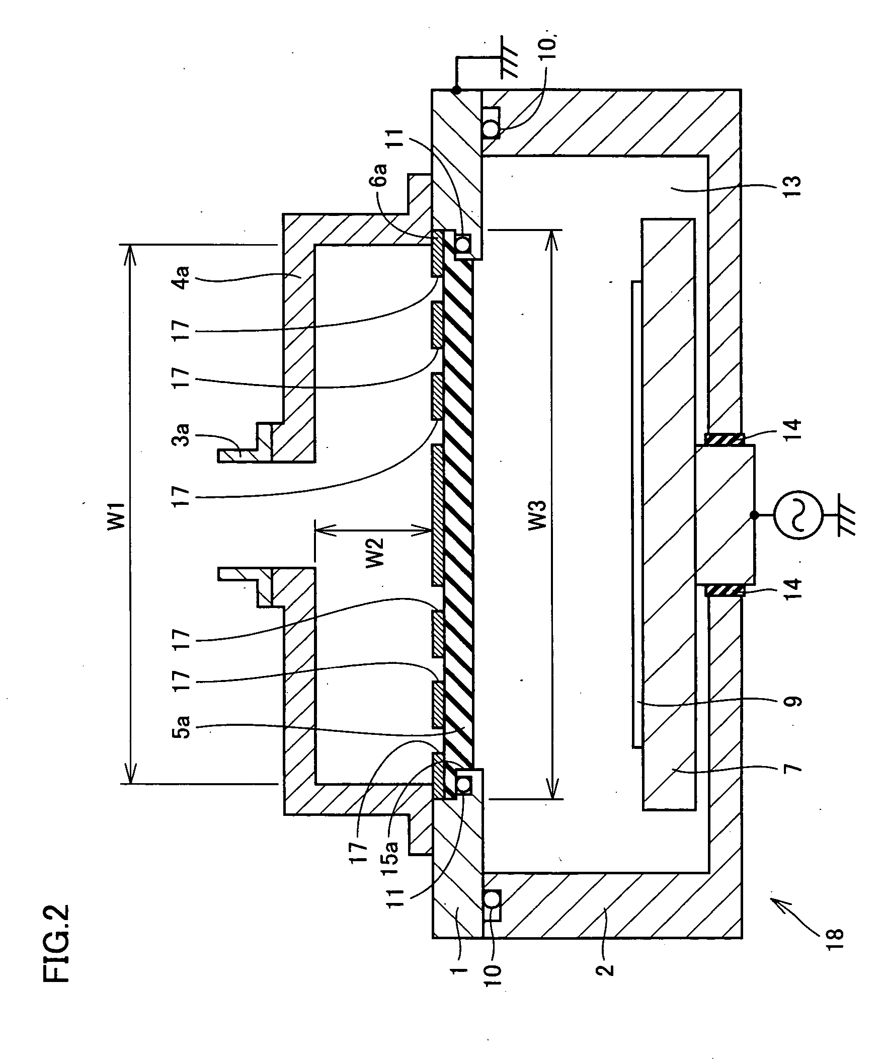
The first embodiment of the plasma processing apparatus according to the present invention is now described with reference to FIGS. 1-3.

Referring to FIGS. 1-3, the plasma processing apparatus 18 is a processing apparatus for performing plasma processing such as film deposition, etching or the like using plasma. Plasma processing apparatus 18 includes a process chamber body 2 made of a member of aluminum or aluminum having coating thereon, a chamber lid 1 arranged on top of process chamber body 2, lead-in waveguides 4a and 4b arranged on top of chamber lid 1, and waveguides 3a and 3b connected to lead-in waveguides 4a and 4b, respectively. Process chamber body 2 and chamber lid 1 constitute a chamber as the processing chamber. A substrate holder 7 for holding a substrate 9 to be processed is arranged in the chamber interior 13. Substrate holder 7 is made of a conductor such as a metal. A stand for supporting substrate holder 7 is provided beneath substrate holder...

second embodiment

(Second Embodiment)

The second embodiment of the plasma processing apparatus according to the present invention is now described with reference to FIG. 5, which corresponds to FIG. 2.

Referring to FIG. 5, the plasma processing apparatus 18 has a structure basically similar to that of the plasma processing apparatus shown in FIGS. 1-3, except for the number and arrangement of dielectrics 19a, 19b. In plasma processing apparatus 18 shown in FIG. 5, two openings 20a, 20b are formed at chamber lid 1 in a region beneath lead-in waveguide 4a, along a longitudinal direction of lead-in waveguide 4a. Dielectrics 19a and 19b are fitted in openings 20a and 20b, respectively. Dielectrics 19a, 19b each have a rectangular shape in cross section in a direction approximately perpendicular to the microwave radiating direction. Similarly, two openings are formed at chamber lid 1 beneath lead-in waveguide 4b (see FIG. 1). Dielectrics having identical shapes to those of dielectrics 19a, 19b of FIG. 5 ...

examples

To confirm the simulated results in the second embodiment described above, two kinds of samples of dielectrics, having thicknesses T of 15.0 mm and 27.5 mm respectively, were prepared as dielectrics 19a, 19b in the plasma processing apparatus shown in FIG. 5. The dielectric samples were placed in plasma processing apparatus 18 separately, and breakdown voltage values were measured. For simulation of the reactant gas, an argon (Ar) gas was supplied to chamber interior 13 at a flow rate of 500 sccm (0.5 l / min) to cause discharge. The results are shown in FIG. 7.

Referring to FIG. 7, the horizontal axis represents a gas pressure of the chamber interior, and the vertical axis represents a microwave power. The solid line represents the lower limit of discharge range (condition range enabling plasma generation) when thickness T of dielectrics 19a, 19b is 15.0 mm. The broken line represents the lower limit of discharge range when thickness T of dielectrics 0.19a, 19b is 27.5 mm.

It is s...


PUM

PropertyMeasurementUnit
pressureaaaaaaaaaa
frequencyaaaaaaaaaa
distanceaaaaaaaaaa

Abstract

A plasma processing apparatus and a processing apparatus having a widened process condition range allowing plasma generation are obtained by increasing microwave propagation efficiency. The plasma processing apparatus includes a processing chamber (1, 2) where plasma processing is performed, and microwave introduction means (3a-6a, 3b-6b, 19a, 19b) for introducing microwaves into the processing chamber. The microwave introduction means (3a-6a, 3b-6b, 19a, 19b) includes a dielectric member (5a, 5b, 19a, 19b) transmitting the microwaves. The dielectric member has a shape in cross section in a direction approximately perpendicular to a transmitting direction of the microwaves through the dielectric member that allows transmission of the microwaves of substantially a single mode. The dielectric member has a thickness T in the transmitting direction that satisfies a condition of (λ×(2m+0.7) / 4)≦T≦(λ×(2m+1.3) / 4), where λ is a wavelength of the microwaves of the single mode transmitted through the dielectric member and m is an arbitrary integer.

Description

DESCRIPTION TECHNICAL FIELD The present invention relates to a plasma processing apparatus and a processing apparatus, and more particularly to a plasma processing apparatus and a processing apparatus utilizing microwaves. BACKGROUND ART Conventionally, plasma processing apparatuses utilizing plasma have been used in manufacturing processes of semiconductor devices and liquid crystal display devices to perform film deposition, etching or the like on substrates thereof. In recent years, with a considerable increase in size of the substrates of the semiconductor devices and the liquid crystal display devices, plasma processing apparatuses capable of processing large-area substrates have been developed. Particularly, with advancement in studies of the use of a rectangular substrate having a size of no smaller than one square meter for the liquid crystal display device, a plasma processing apparatus capable of processing such a large-size substrate has been developed. One of the most ...

Claims


Application Information

Patent Timeline
Patent Type & Authority Applications(United States)
IPC IPC(8): H05H1/46C23C16/511H01J37/32H01L21/205H01L21/302H01L21/3065
CPCH01J37/32238H01J37/32192
Inventor YAMAMOTO, NAOKOYAMAMOTO, I'ATSUSHIHIRAYAMA, MASAKIOHMI, I'ADAHIRO
Owner SHARP KK
Why Eureka
Try Eureka