Wafer probe for measuring plasma and surface characteristics in plasma processing environments

a plasma processing environment and surface characteristics technology, applied in the field of plasma processing environments, can solve the problems of limiting the use of measuring devices for real-time affecting the accuracy of plasma and substrate temperature measurement, and inconvenient operation, so as to reduce or avoid the effect of averaged measurements taken in pulsed plasma environment and limited onboard memory and power resources

Inactive Publication Date: 2005-01-20
KLA TENCOR TECH CORP
View PDF30 Cites 47 Cited by
  • Summary
  • Abstract
  • Description
  • Claims
  • Application Information

AI Technical Summary

Benefits of technology

In one embodiment of the invention, a sensor probe apparatus comprises sensors that detect triggering events for gating and synchronization of other probe sensors in a pulsed plasma processing system. By triggering sensors on specific physical events of the plasma, noise or aliasing associated with un-gated, averaged measurements taken in a pulsed plasma environment can be reduced or avoided. In addition, gating and synchronization of data collection conserves the limited onboard memory and power resources that may be available in an in-situ diagnostic probe device.

Problems solved by technology

However, all the examples of the prior art have several limitations that restrict their use for obtaining real-time plasma and substrate temperature measurement within a plasma processing system.
Many of these measuring devices are intrusive in that they require the use of wires into the plasma processing system and others are passive recording devices that cannot make real-time measurements.
Also, those devices that do not use external wires are limited in on-time operation and power supply current draw since they rely entirely upon on-board battery power sources that have limited milliamp-per-hour capacity or limited sustainable trickle current capacity when attempting to power a sizable array of sensors, microprocessor(s) and wireless communication subsystems.
Moreover, in the context of these in situ measurement apparatuses, none of the prior art teachings discuss in detail how to devise a sensor capable of obtaining plasma measurements, such as charged-particle (ion or electron) fluxes, densities and energies that can be adapted to a wireless sensing apparatus.

Method used


Image

  • Wafer probe for measuring plasma and surface characteristics in plasma processing environments
  • Wafer probe for measuring plasma and surface characteristics in plasma processing environments
  • Wafer probe for measuring plasma and surface characteristics in plasma processing environments

Examples


Embodiment Construction

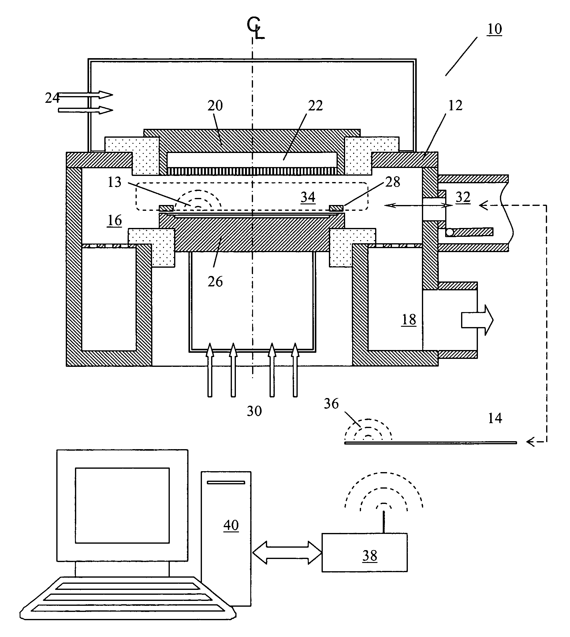
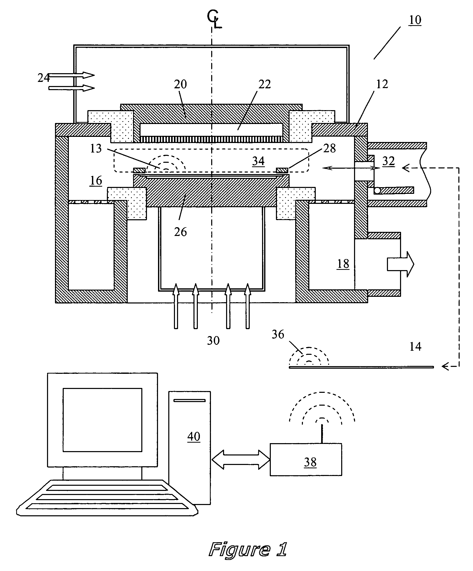
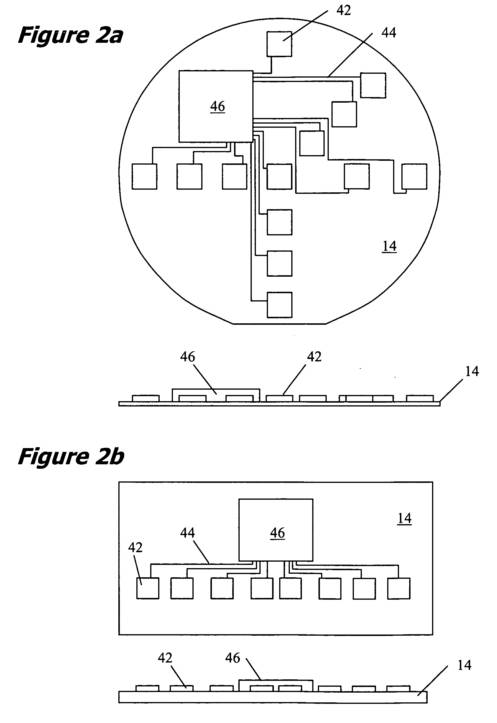
Referring to FIG. 1 there is illustrated an apparatus 10 that is capable of making real-time measurements of incident plasma current flux and surface temperatures of a work piece in a plasma processing system 12. In this particular illustration a diagnostic probe 14 is comprised of a silicon wafer substrate that incorporates plasma probe and surface temperature diagnostic circuitry and wireless communications and a stored power system. In the preferred embodiment, the probe 14 is powered up outside the plasma processing system 12 to enable diagnostic communications prior to use for real-time measurements. The plasma processing system of FIG. 1 is one of many possible plasma processing systems and is presented here to illustrate the function and use of the present invention. The processing system is comprised of a vacuum processing chamber 16, a pumping manifold 18, a plasma source electrode mounted to the top of the chamber 20, a gas delivery manifold or gas shroud 22, gas flow and...


PUM

PropertyMeasurementUnit
diameteraaaaaaaaaa
diameteraaaaaaaaaa
plasma propertiesaaaaaaaaaa

Abstract

There is provided by this invention a wafer probe for measuring plasma and surface characteristics in plasma processing environment that utilizes integrated sensors on a wafer substrate. A microprocessor mounted on the substrate receives input signals from the integrated sensors to process, store, and transmit the data. A wireless communication transceiver receives the data from the microprocessor and transmits information outside of the plasma processing system to a computer that collects the data during plasma processing. The integrated sensors may be dual floating Langmuir probes, temperature measuring devices, resonant beam gas sensors, optical emission sensors, or other sensors of plasma or surface properties. There is also provided a self-contained power source that utilizes the plasma for power that is comprised of a topographically dependent charging device or a charging structure that utilizes stacked capacitors.

Description

BACKGROUND OF THE INVENTION 1. Field of the Invention This invention relates generally to apparatus and methods in which surface-based sensors measure incident charged-particle currents, charging voltages, temperatures and other physical parameters at a work piece surface during plasma processing, and more particularly to a semiconductor wafer utilizing surface-based sensors to provide real time measurement of plasma characteristics adjacent to the wafer surface as well as select physical properties during plasma processing. 2. Brief Description of the Prior Art Spatial and temporal variation in plasma characteristics and the work piece surface temperature can strongly influence the performance and yield of plasma-based processes, such as those encountered in semiconductor manufacture. In such processes, variations in physical plasma parameters that occur adjacent to the process work piece directly impact process metrics which may include the following: (1) etch rates and etch p...

Claims


Application Information

Patent Timeline
Patent Type & Authority Applications(United States)
IPC IPC(8): H01J37/32H01L21/00
CPCH01L21/67253H01J37/32935
Inventor MAHONEY, LEONARD J.CARTER, DANIEL C.ROBERTS, STEVEN J.ROCHE, GREGORY A.
Owner KLA TENCOR TECH CORP
Why Eureka
Try Eureka