Method and apparatus of forming alignment film

a technology of alignment film and alignment film, which is applied in the direction of mechanical equipment, machines/engines, instruments, etc., can solve the problems of high manufacturing cost, many critical problems in conventional manufacturing processes, so as to improve the alignment of liquid crystal molecules and reduce the time for forming alignment films

Inactive Publication Date: 2005-01-20
SAMSUNG DISPLAY CO LTD
View PDF2 Cites 17 Cited by
  • Summary
  • Abstract
  • Description
  • Claims
  • Application Information

AI Technical Summary

Benefits of technology

[0029] According to the present invention, the alignment film is formed on the thin film transistor unit cell and on the color filter unit cel

Problems solved by technology

However, the conventional manufacturing processes has some critical problems.
However, the greater the number of the equipment is, the higher is the manufacturing cost.
Further, the conventional manufacturing processes have many problems.
A first problem occurs in the rubbing process.
The particles may induce failures during the rubbing process.
Therefore, the conventional rubbing process cannot be successfully performed and the efficiency of manufacturing the liquid crystal display device is lowered.
Therefore, defects of the alignment grooves are seldom detected, when the alignment grooves are already formed.
The defects of the alignment grooves may be detected in the reliabil

Method used


Image

  • Method and apparatus of forming alignment film
  • Method and apparatus of forming alignment film
  • Method and apparatus of forming alignment film

Examples


first embodiment

OF A NON-CONTACT TYPE ALIGNMENT OF LIQUID CRYSTAL MOLECULES

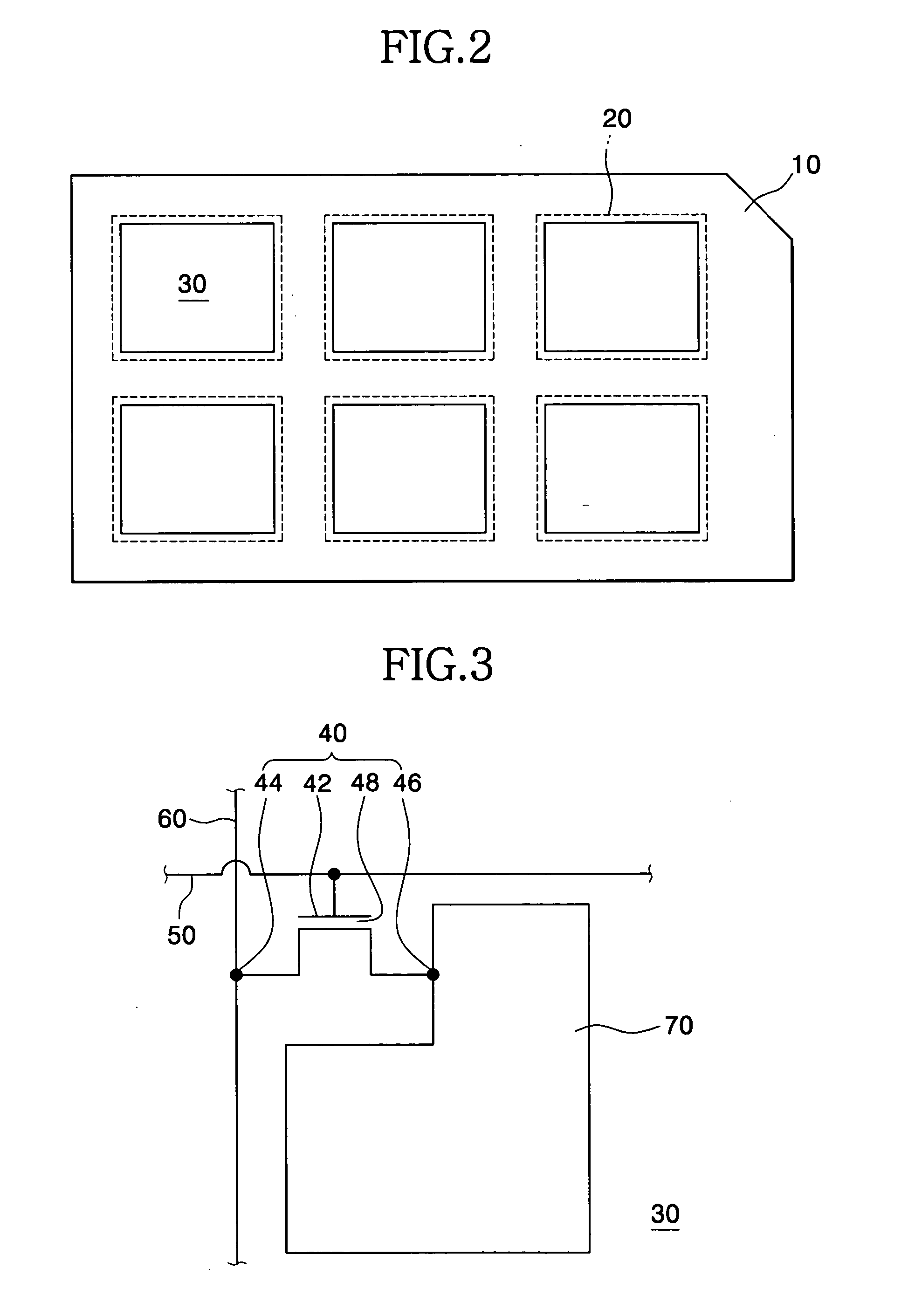
[0100] In order to align liquid crystal molecules on the thin film transistor unit cell 30 of FIG. 2 or on the color filter unit cell 100 of FIG. 5, an alignment film and an atomic beam to be applied to the alignment film are needed.

[0101]FIG. 7 is a cross-sectional view showing an alignment film formed on the first mother substrate or the second mother substrate according to the first exemplary embodiment.

[0102] Referring to FIG. 7, an alignment film 130 includes a diamond-like-carbon thin film (DLC film) formed on surfaces of the thin film transistor unit cell and on the color filter unit cell. The alignment film 130 may include SiO2, Si3N4 and TiO2 aside from the diamond-like-carbon thin film.

[0103] Hereinafter, the diamond-like-carbon thin film is referenced by the reference numeral 130.

[0104] The diamond-like-carbon thin film 130 is used as an alignment film because the diamond-like-carbon thin film 130 has a carbon...

second embodiment

OF A NON-CONTACT TYPE ALIGNMENT OF LIQUID CRYSTAL MOLECULES

[0167]FIG. 13 is a flow chart showing a method of aligning liquid crystal by a non-contact method according to a second exemplary embodiment.

[0168] In previous procedure, the diamond-like-carbon thin film having a carbon-carbon double bond is formed on the first substrate 10 having the thin film transistor unit cell 30 of FIG. 2 or on the second substrate 80 having the color filter unit cell 100 of FIG. 5. The diamond-like-carbon thin film is formed via Chemical Vapor Deposition (CVD).

[0169] Referring to FIG. 13, the atomic beam collides with the diamond-like-carbon thin film, so that a polarized functional group for aligning liquid crystal molecules is generated (step S225).

[0170]FIG. 14 is a flow chart showing a method of generating a polarized functional group in the diamond-like-carbon thin film according to the second exemplary embodiment.

[0171] Referring to FIG. 14, a first ion beam is generated and accelerated tow...

third embodiment

OF A NON-CONTACT TYPE ALIGNMENT OF LIQUID CRYSTAL MOLECULES

[0188]FIG. 16 is a flow chart showing a process of introducing a hydrogen ion into the polarized functional group according to a third exemplary embodiment of the present invention.

[0189] Deionized water is supplied to the surface of the diamond-like-carbon thin film in order that hydrogen ion (H+) is combined with the sub-chain (step S233).

[0190] Then, ultra-violet ray is irradiated onto the surface of the diamond-like-carbon thin film in order that the hydrogen ion (H+) is combined with the sub-chain (step S234).

[0191] When the ultra-violet ray is irradiated on the deionized water, two hydrogen ions and one oxygen ion are generated as shown in the following chemical formula.

H2O→2H++O−2   

[0192] The hydrogen ion (H+) dissociated by the ultra-violet ray is combined with the sub-chain to form a C—H bond.

[0193] When the hydrogen ion (H+) is combined with the sub-chain formed in the diamond-like-carbon thin film in which t...


PUM

PropertyMeasurementUnit
Temperatureaaaaaaaaaa
Pressureaaaaaaaaaa
Polarityaaaaaaaaaa

Abstract

In a method of manufacturing an LCD device, an atomic beam is irradiated onto a thin film including a carbon-carbon double bond to form a polarized functional group by transforming the carbon-carbon double bond into a carbon-carbon single bond and a radical state. Then, a polarity preserving material is combined with the polarized functional group so as to preserve a polarity of the polarized functional group. According to the present invention, the alignment film is formed on the thin film transistor unit cell and on the color filter unit cell by a non-contact method. Therefore, time of forming the alignment film is reduced and alignment of the liquid crystal molecules is improved.

Description

CROSS-REFERENCE TO RELATED APPLICATIONS [0001] This application relies for priority upon Korean Patent Application No.2002-74478 filed on Nov. 27, 2002, the contents of which are herein incorporated by reference in its entirety. BACKGROUND OF THE INVENTION [0002] 1. Field of the Invention [0003] The present invention relates to a method and an apparatus of forming an alignment film, and more particularly to a non-contacting method and an apparatus of forming an alignment film. [0004] 2. Description of the Related Art [0005] In general, a liquid crystal display device is lighter and smaller than other display devices comparatively. The liquid crystal display devices are manufactured via many manufacturing processes. [0006] A first process for manufacturing the liquid crystal display device includes a forming of thin film transistor (TFT) unit cells on a first mother substrate and a forming of color filter unit cells on a second mother substrate. One example of the first process for m...

Claims


Application Information

Patent Timeline
IPC IPC(8): C23C16/26C23C16/56F01P3/02F01L1/34G02F1/1337
CPCC23C16/26C23C16/56G02F2001/133765G02F1/133788G02F1/13378G02F1/133765G02F1/1337
Inventor CHOO, DAE-HOKIM, HAK-JINLEE, BONG-WOO
Owner SAMSUNG DISPLAY CO LTD
Why Eureka
Try Eureka