Cutting method and method of manufacturing semiconductor device

a technology of cutting method and manufacturing method, which is applied in the direction of semiconductor devices, semiconductor/solid-state device details, electrical equipment, etc., can solve the problems of increasing the manufacturing defects of semiconductor devices, affecting the performance of semiconductor devices, and causing excessive material on the cut cross-section, etc., to achieve the effect of removing burrs

Active Publication Date: 2005-01-20
SEMICON COMPONENTS IND LLC
View PDF1 Cites 10 Cited by
  • Summary
  • Abstract
  • Description
  • Claims
  • Application Information

AI Technical Summary

Benefits of technology

[0011] In light of the above, it is an object of the present invention to provide a cutting method capable of effectively removing burrs.
[0014] It is possible according to the present invention to remove burrs in a first layer having a ductile property when the first and second layers are cut. Thus, the present invention allows provision of a cutting method capable of effectively removing burrs.

Problems solved by technology

While a soft and ductile metal material such as copper or aluminum is cut in the aforementioned cutting steps, it is known that cutting such a metal material produces burrs (excess material, debris) on the cut cross-sections.
In this case it is possible that electrodes (bonding pads) arranged at the perimeter portion of the chip front surface or electrodes (external terminals) arranged at the perimeter portion of the package mounting surface could be short-circuited via the produced burrs, thus resulting in increased manufacturing defects of semiconductor devices.
Further, fine pitch techniques are increasingly used as a result of recent trends toward downsizing and thickness reduction of semiconductor devices, possibly resulting in aggravating the aforementioned problem if burrs are produced between reduced pitch spacings.

Method used


Image

  • Cutting method and method of manufacturing semiconductor device
  • Cutting method and method of manufacturing semiconductor device
  • Cutting method and method of manufacturing semiconductor device

Examples


Embodiment Construction

[0032] An embodiment of the present invention will be described hereinbelow with reference to the drawings.

[0033]

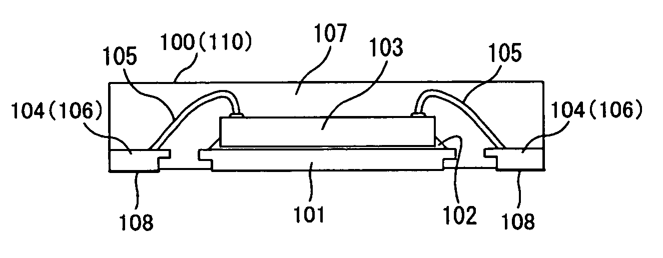
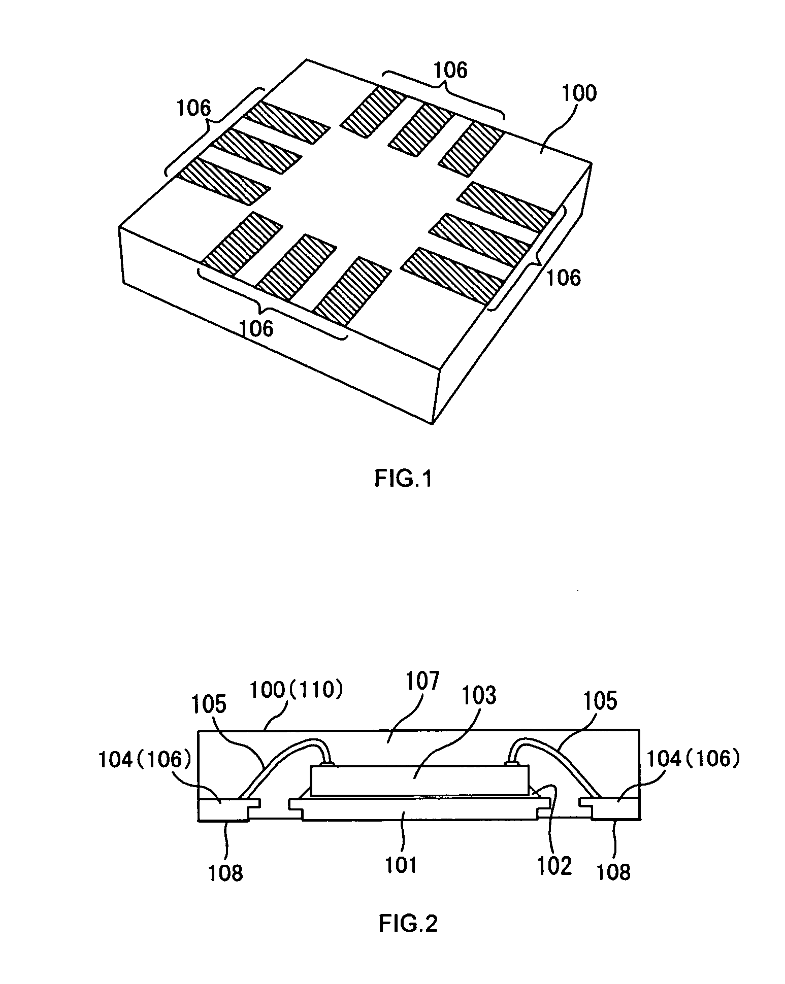
[0034]FIG. 1 is a perspective view showing an embodiment of a semiconductor device 100 manufactured based on a cutting method according to the present invention.

[0035] As the semiconductor device 100 according to the present invention, a nonleaded semiconductor device such as VQFN (Very thin Quad Flat Nonleaded Package) or VSON (Very Thin Small Outline Nonleaded Package) may be used, as shown in the same figure, in which external terminals 106 are exposed from the mounting surface (bottom surface), a surface that is joined to a printed circuit board via a joining agent. It is needless to say that the semiconductor device 100 according to the present invention is not limited to nonleaded semiconductor devices and that other CSPs (Chip Size Packages) such as BGA (Ball Grid Array) may be used. Package employing a printed circuit board or flexible printed board may also be ...


PUM


Abstract

A cutting method for separating individual semiconductor devices by cutting boundary portions in a group of semiconductor devices made up by arranging a plurality of semiconductor devices in which a ductile first layer and a second layer are stacked on a peripheral side thereof, the cutting method comprises a cutting step of cutting the first and second layers by moving a first rotary body from the boundary portions of the group of semiconductor devices in the direction in which the first and second layers are stacked; and a burr removal step of removing burrs from the first layer by moving a second rotary body, softer than the first rotary body and wider than the first rotary body in the direction of rotational axis, from the cut boundary portions of the group of semiconductor devices in the direction in which the first and second layers are stacked.

Description

CROSS-REFERENCE TO RELATED APPLICATIONS [0001] The present application claims priority upon Japanese Patent Application No. 2003-275400 filed on Jul. 16, 2003, which is herein incorporated by reference. BACKGROUND OF THE INVENTION [0002] 1. Field of the Invention [0003] The present invention relates to a cutting method and a method of manufacturing a semiconductor device, capable of effectively removing burrs. [0004] 2. Description of the Related Art [0005] In semiconductor device manufacturing steps, steps are performed such as a cutting step of separating each partitioned region (chip: “semiconductor device”), in which a given circuit pattern is formed on a semiconductor wafer (“group of semiconductor devices”), using a cutting device called dicer or dicing, (See Japanese Patent Application Laid-open Publication No. 2001-77055), and a cutting step of separating each partitioned region (package: “semiconductor device”) from a leadframe (“group of semiconductor devices”) in plate fo...

Claims


Application Information

Patent Timeline
Patent Type & Authority Applications(United States)
IPC IPC(8): H01L21/301H01L21/48H01L21/56H01L21/68H01L23/31
CPCH01L21/4842H01L21/561H01L2924/10253H01L2224/49171H01L2924/01006H01L2224/48247H01L2224/32245H01L24/48H01L2924/18301H01L2924/01082H01L2924/01079H01L2924/01078H01L2924/01047H01L2924/01033H01L2924/0103H01L2924/01029H01L2924/01013H01L2224/97H01L2224/73265H01L2224/48465H01L2224/48091H01L2221/68331H01L24/97H01L23/3107H01L21/6835H01L2224/85H01L2924/00014H01L2224/83H01L2924/00012H01L2924/00H01L24/49H01L24/73H01L2924/181H01L2224/45099H01L2224/45015H01L2924/207
Inventor KAMEYAMA, KOUJIROMITA, KIYOSHI
Owner SEMICON COMPONENTS IND LLC
Why Eureka
Try Eureka